A dream of scientists has been to visualise details of structures within our cells in real time, a breakthrough that would greatly aid in the study of their function. However, even the best of current microscopes can take minutes to recreate images of the internal machinery of cells at a usable resolution.
Thanks to a technical tour de force, involving new algorithms, Yale University researchers can now generate accurate images of sub-cellular structures in milliseconds, rather than minutes. This could be of great help in the study of cancer and other diseases. Below is an image of microtubules, which act as cellular scaffolding, captured in just 33 milliseconds using video-rate nanoscopy.
“We can now see research come to life and tackle complex questions or conditions which require hundreds of images, something we have not been able to do before,” said Joerg Bewersdorf, assistant professor of cell biology and biomedical engineering and senior author of the research, published in the journal Nature Methods.
Cameras will soon take clear and sharp photos even in dim conditions, thanks to a revolutionary new sensor invented at Nanyang Technological University (NTU).
The new sensor – made from graphene – is believed to be the first to be able to detect broad spectrum light, from the visible to mid-infrared, with high photoresponse or sensitivity. This means it is suitable for use in all types of cameras, including infrared, traffic speed cameras, satellite imaging and more.
Not only is the graphene sensor 1,000 times more sensitive to light than current low-cost imaging sensors found in today’s compact cameras, it also uses 10 times less energy as it operates at lower voltages. When mass produced, graphene sensors are estimated to cost at least five times cheaper.
Graphene is a million times smaller than the thickest human hair (only one-atom thick) and made of pure carbon atoms arranged in a honeycomb structure. It is known to have a high electrical conductivity among other properties such as durability and flexibility.
Assistant Professor Wang Qijie, from NTU’s School of Electrical & Electronic Engineering, said: “We have shown that it is now possible to create cheap, sensitive and flexible photo sensors from graphene alone. We expect our innovation will have great impact not only on the consumer imaging industry, but also in satellite imaging and communication industries, as well as the mid-infrared applications.
“While designing this sensor, we have kept current manufacturing practices in mind. This means the industry can in principle continue producing camera sensors using the CMOS (complementary metal-oxide-semiconductor) process, which is the prevailing technology used by the majority of factories in the electronics industry. Therefore manufacturers can easily replace the current base material of photo sensors with our new nano-structured graphene material.”
Fabrication process of the device. Credit: Y. Z. Zhang et al./Nature Communications
Asst Prof Wang came up with an innovative idea to create nanostructures on graphene which “trap” light-generated electron particles for a much longer time, resulting in a stronger electric signal. Such electric signals can then be processed into an image, like a photograph captured by a digital camera.
The “trapped electrons” is key to achieving high photoresponse in graphene, which makes it far more effective than traditional CMOS or CCD (charge-coupled device) image sensors, said Wang. Essentially, the stronger the electric signals being generated, the clearer and sharper the photos.
“The performance of our graphene sensor can be further improved, such as the response speed, through nanostructure engineering of graphene, and preliminary results already verified the feasibility of our concept,” he added.
The research, costing $200,000, took Wang and his colleagues a total of two years to complete. The next step is to work with industry collaborators to develop the sensor into a commercial product.
Every chemist’s dream – to capture an atomic-scale picture of a chemical before and after it reacts – has now come true, thanks to a new technique developed by researchers at the University of California.
Using a state-of-the-art, atomic force microscope, the scientists have taken the first atom-by-atom pictures, including images of the chemical bonds between atoms, clearly depicting how a molecule's structure changed during a reaction. Until now, scientists have only been able to infer this type of information from spectroscopic analysis.
“Even though I use these molecules on a day to day basis, actually being able to see these pictures blew me away. Wow!” said lead researcher Felix Fischer, UC Berkeley assistant professor of chemistry. “This was what my teachers used to say that you would never be able to actually see, and now we have it here.”
The ability to image molecular reactions in this way could help not only students as they study chemical structures and their reactions, but will also show chemists the products of their experiments and help them fine-tune the reactions to get the results they want. Fischer, along with Professor Michael Crommie, captured these images with the goal of building new graphene nanostructures – a hot area of research today for their potential in next-generation computers.
However, the implications go far beyond just graphene, Fischer said. This technique will find application in the study of heterogeneous catalysis, for example, which is used widely in the oil and chemical industries. Heterogeneous catalysis involves the use of metal catalysts like platinum to speed up reactions, as in the catalytic converter of a car.
“To understand the chemistry that is actually happening on a catalytic surface, we need a tool that is very selective and tells us which bonds have actually formed and which ones have been broken,” Fischer explained. “This technique is unique out there right now for the accuracy with which it gives structural information. I think it’s ground-breaking.”
“The atomic force microscope gives us new information about the chemical bond, which is incredibly useful for understanding how different molecular structures connect up, and how to convert from one shape into another shape,” said Crommie. “This should help us to create new engineered nanostructures – such as bonded networks of atoms that have a particular shape and structure for use in electronic devices. This points the way forward.”
Traditionally, researchers conduct detailed analyses to determine the products of a chemical reaction – and even then, the actual 3-D arrangement of atoms in these products can be ambiguous.
“In chemistry, you throw stuff into a flask and something else comes out, but you typically only get very indirect information about what you have,” Fischer said. “You have to deduce that by taking nuclear magnetic resonance, infrared or ultraviolet spectra. It is more like a puzzle, putting all the information together and then nailing down what the structure likely is. But it's just a shadow. Here, we actually have a technique at hand where we can look at it and say this is exactly the molecule. It’s like taking a snapshot of it.”
Working together, Fischer and Crommie devised a way to chill the reaction surface and molecules to the temperature of liquid helium, which stops them from jiggling around. They then used a scanning tunnelling microscope to locate all the molecules on the surface, and zeroed in on several to probe more finely with the atomic force microscope. To enhance the spatial resolution, they put a single carbon monoxide molecule on the tip. After imaging the molecule, they heated the surface until the molecule reacted, then again chilled the surface and imaged the reaction products.
Non-contact atomic force microscope (nc-AFM) images (centre) of a molecule before and after a reaction improve immensely over images (top) from a scanning tunnelling microscope and look just like the classic molecular structure diagrams (bottom).
Solar engineers from the University of New South Wales (UNSW) have developed a new method to dramatically improve the quality of low-grade silicon, boost electrical efficiency and reduce the cost of solar panels.
The UNSW team has discovered a mechanism to control hydrogen atoms so they can better correct deficiencies in silicon – by far the most expensive component used in the making of solar cells.
"This process will allow lower-quality silicon to outperform solar cells made from better-quality materials," says Scientia Professor Stuart Wenham from the School of Photovoltaics and Renewable Energy Engineering.
Standard commercial silicon cells currently have a maximum efficiency of around 19%. The new technique, patented by UNSW researchers earlier this year, is expected to produce efficiencies between 21% and 23%, says Wenham.
"By using lower-quality silicon to achieve higher efficiencies, we can enable significant cost reductions," he says.
The solar industry has long been focused on bringing down the cost of silicon. However, cheaper silicon also means lower-quality silicon, with more defects and contaminants that reduce efficiency.
It's been known for several decades that hydrogen atoms can be introduced into the atomic structure of silicon to help correct these defects, but until now, researchers had limited success in controlling the hydrogen to maximise its benefits or even understanding why this happens.
Atomic structure of silicon.
"Our research team has worked out how to control the charge state of hydrogen atoms in silicon – something that other people haven't previously been able to do," says Wenham.
Hydrogen atoms can exist in three 'charge' states – positive, neutral and negative. The charge state determines how well the hydrogen can move around the silicon and its reactivity, which is important to help correct the defects.
"We have seen a 10,000 times improvement in the mobility of the hydrogen and we can control the hydrogen so it chemically bonds to things like defects and contaminants, making these inactive," says Wenham.
The UNSW team currently has eight industry partners interested in commercialising the technology, and is also working with manufacturing equipment companies to implement the new capabilities.
The project, which has been generously supported by the Australian Renewable Energy Agency, is expected to be completed in 2016.
UNSW still holds the world-record for silicon cell efficiency at 25%, and last week, Scientia Professor and solar pioneer Martin Green, was elected into the Fellowship of the United Kingdom's prestigious Royal Society.
Researchers in Spain have managed to give graphene magnetic properties. This breakthrough, published in the journal Nature Physics, opens the door to the development of graphene-based spintronic devices; that is, devices based on the spin or rotation of the electron, which could transform the electronics industry.
TCNQ molecules on graphene layer, where they acquire a magnetic order. Credit: IMDEA-Nanoscience
Scientists were already aware that graphene, an incredible material formed of a mesh of hexagonal carbon atoms, has extraordinary conductivity, mechanical and optical properties. Now it is possible to give it yet one more property: magnetism, implying a breakthrough in electronics.
This is revealed in a study that the Madrid Institute for Advanced Studies in Nanoscience (IMDEA-Nanociencia) and Autonoma Autonomous (UAM) and Complutense (UCM) universities of Madrid have just published in Nature Physics. Researchers managed to create a hybrid surface from this material that behaves as a magnet.
Prof. Rodolfo Miranda, Director of IMDEA-Nanociencia: "In spite of the huge efforts to date of scientists all over the world, it has not been possible to add the magnetic properties required to develop graphene-based spintronics. However, these results pave the way to this possibility."
Spintronics is based on the charge of the electron, as in traditional electronics, but also on its "spin", which determines its magnetic moment. Material is magnetic when most of its electrons have the same spin. As the spin can have two values, its use adds two more states to traditional electronics. This positioning can be translated into a binary signal (1 or 0). Thus, both data processing speed and quantity of data to be stored on electronic devices can be increased, with applications in fields such as telecommunications, computing, energy and biomedicine.
A TCNQ molecule on the graphene mesh which in turn has been
grown on a ruthenium crystal. Credit: IMDEA-Nanoscience
In order to develop a graphene-based spintronic device, the challenge was to 'magnetise' the material, and researchers from Madrid found how through the quantum and nanoscience world. The technique involved growing an ultra-precise graphene film over a ruthenium single crystal, inside an ultra-high vacuum chamber where organic molecules of tetracyano-p-quinodimethane (TCNQ) are evaporated on the graphene surface. TCNQ is a molecule that acts as a semiconductor at very low temperatures in certain compounds.
On observing results through a scanning tunnelling microscope (STM), scientists were surprised: organic molecules had organised themselves and were regularly distributed all over the surface, interacting electronically with the graphene-ruthenium substrate.
"We have proved in experiments how the structure of the TCNQ molecules over graphene acquires long-range magnetic order, with electrons positioned in different bands according to their spin," clarifies Prof. Amadeo Vázquez de Parga.
Meanwhile, his colleague Prof. Fernando Martin has conducted modelling studies that have shown that, although graphene does not interact directly with the TCNQ, it does permit a highly efficient charge transfer between the substrate and the TCNQ molecules and allows the molecules to develop long-range magnetic order.
The result is a new graphene-based magnetised layer, which paves the way towards the creation of devices based on what was already considered as the material of the future, but which now may also have magnetic properties.
In a new study performed by the Center for Nanoscale Materials at the U.S. Department of Energy's (DOE) Argonne National Laboratory, researchers have for the first time seen the self-assembly of nanoparticle chains in situ, that is, in place as it occurs in real-time.
The scientists exposed a tiny liquid "cell" or pouch that contained gold nanoparticles covered with a positively charged coating to an intense beam of electrons generated with a transmission electron microscope. Some of the electrons that penetrated the outside of the cell became trapped in the fluid medium in the cell. These "hydrated" electrons attracted the positively charged nanoparticles, which in time reduced the intensity of charge of the positive coating.
As the hydrated electrons reduced the coating's positive charge, the nanoparticles no longer repelled each other as strongly. Instead, their newfound relative attraction led the nanoparticles to "jump around" and eventually stick together in long chains. This self-assembly of nanoparticle chains had been detected before in different studies, but this technique allowed researchers, for the first time, to observe the phenomenon as it occurred.
"The moment-to-moment behaviour of nanoparticles is something that's not yet entirely understood by the scientific community," said Argonne nanoscientist Yuzi Liu, the study's lead author. "The potential of nanoparticles in all sorts of different applications and devices — from tiny machines to harvesters of new energy sources — requires us to bring all of our resources to bear to look at how they function on the most basic physical levels."
Self-assembly is particularly interesting to scientists because it could lead to new materials that could be used to develop new, energy-relevant technologies. "When we look at self-assembly, we're looking to use nature as a springboard into man-made materials," said Tijana Rajh, who directed the group that carried out the study.
Because the particles under study were so tiny — just a few dozen nanometers in diameter — an optical microscope would not have been able to resolve, or see, individual nanoparticles. By using the liquid cell in the transmission electron microscope at the Center for Nanoscale Materials, Liu and his colleagues could create short movies showing the quick movement of the nanoparticles as their coatings contacted the hydrated electrons.
Researchers at the University of Illinois have developed a new type of battery that could revolutionise the way consumer electronics and electric vehicles are powered.
Led by William King, the Bliss Professor of mechanical science and engineering, the researchers published their results in Nature Communications. They describe a new class of "microbatteries" which owe their high performance to an internal three-dimensional microstructure.
"The thinking parts of computers have gotten small," said King. "And the battery has lagged far behind. This is a microtechnology that could change all of that. Now, the power source is as high-performance as the rest of it."
Batteries have two key components: the anode (minus side) and cathode (plus side). Building on a novel fast-charging cathode design by materials science and engineering professor Paul Braun's group, King and his colleague James Pikul developed a matching anode, then developed a new way to integrate the two components at the microscale to make a complete battery with superior performance.
"Our key insight," they report, "is that the battery micro-architecture can concurrently optimize ion and electron transport for high-power delivery, realized here as three-dimensional bi-continuous interdigitated microelectrodes. The battery microarchitecture affords trade-offs between power and energy density, resulting in a high-performance power source which is scalable to larger areas."
With so much raw power, the batteries could enable sensors that broadcast 30 times farther, or devices 30 times smaller. The batteries are rechargeable and can charge 1,000 times faster than competing technologies, potentially allowing a smartphone to be replenished in a matter of seconds. As well as consumer electronics, a vast range of other applications could benefit – from tiny medical devices, up to large objects like electric vehicles.
The team is now working on integrating their batteries with other components and will begin trials on electronic equipment before the end of the year. Safety issues will also need to be resolved, as well as manufacturability at low cost. However, this appears to be a very promising development.
An advance in micromotors, akin to the invention of cars that fuel themselves from the pavement or air, rather than gasoline or batteries, could lead to a range of new medical and industrial uses for these tiny devices.
Scientists revealed their latest breakthroughs in New Orleans yesterday, as part of the 245th National Meeting & Exposition of the American Chemical Society. Joseph Wang, who leads research on the motors, said that efforts to build tiny self-powered robot devices – so small that thousands would fit inside this "o" – have evoked memories of the 1966 science fiction film Fantastic Voyage. That movie featured a miniaturised submarine, which doctors injected into a patient. It then navigated through blood vessels to remove a blood clot in the brain.
Fuel and propulsion systems have been a major barrier in moving science fiction closer to practical reality, Wang explained. Some micromotors and even-smaller nanomotors, for instance, have relied on hydrogen peroxide fuel, which could damage body cells. Others have needed complex magnetic or electronic gear to guide their movement.
"We have developed the first self-propelled micromotors and microrockets that use the surrounding natural environment as a source of fuel," he said. "The stomach, for instance, has a strongly acid environment that helps digest food. Some of our microrockets use that acid as fuel, producing bubbles of hydrogen gas for thrust and propulsion. The use of biocompatible fuels is attractive for avoiding damage to healthy tissue in the body. We envision that these machines could someday perform microsurgery, clean clogged arteries or transport drugs to the right place in the body. But there are also possible uses in cleaning up oil spills, monitoring industrial processes and in national security."
Wei Gao, a graduate student in Wang's lab, described how the team at the University of California, San Diego, has developed two types of self-propelled vehicles – microrockets made of zinc and micromotors made of aluminium. The tubular zinc micromotor is one of the world's fastest, able to move 100 times its 0.0004-inch length in just one second. That's like a sprinter running 400 miles per hour. The zinc lining is biocompatible. It reacts with the hydrochloric acid in the stomach, which consists of hydrogen and chloride ions. It releases the hydrogen gas as a stream of tiny bubbles, which propel the motor forward. This rocket would be ideal to deliver drugs or to capture diseased cells in the stomach, according to Gao.
Gao also described some of the latest advances in the technology. The newest vehicles are first-of-their-kind aluminium micromotors. One type, which also contains gallium, uses water as a fuel. It splits water to generate hydrogen bubbles, which move the motor. "About 70 percent of the human body is water, so this would be an ideal fuel for vehicles with medical uses, such as microsurgery," said Wang. "They could also have uses in clinical diagnostic tests, in the environment and in security applications."
Another type of aluminium micromotor doesn't have gallium and is the first such motor that can use multiple fuels. "We're really excited about this micromotor," said Gao. "It is our most flexible one to date. For the first time, we've made a micromotor that can use three different fuels – acids, bases and hydrogen peroxide, depending upon its surroundings. Therefore, we can use these motors in many more environments than ever before."
The scientists are working on extending the lifetimes of these vehicles so that they last longer and functionalising them for specific biomedical applications. They are also exploring commercial partners for realising real-life applications of this work.
The defence contractor, Lockheed Martin, has reported a new method for desalination that is vastly cheaper and more efficient, using nanotechnology.
Lockheed Martin has been awarded a patent for "Perforene" – a new molecular filtration system that is designed to meet the growing global demand for potable water. This material works by removing sodium, chlorine and other ions from seawater and other sources.
Dr. Ray Johnson, senior vice president and chief technology officer: "Access to clean drinking water is going to become more critical as the global population continues to grow, and we believe that this simple and affordable solution will be a game-changer for the industry. Perforene ... is just one example of Lockheed Martin's efforts to apply some of the advanced materials that we have developed for our core markets, including aircraft and spacecraft, to global environmental and economic challenges."
According to a UN report last year, over 780 million people around the world do not have access to clean drinking water. Tom Notaro, Lockheed business manager for advanced materials: "One of the areas that we're very concerned about in terms of global security is the access to clean and affordable drinking water. As more and more countries become more developed ... access to that water for their daily lives is becoming more and more critical."
Perforene was developed by placing holes that are one nanometre or less in a membrane of graphene. These are small enough to trap ions while dramatically improving the flow-through of water molecules, reducing clogging and pressure. Being just one atom thick, graphene is both strong and durable, making it far more effective at sea water desalination at a fraction of the cost of traditional reverse osmosis systems.
John Stetson, senior engineer: "It's 500 times thinner than the best filter on the market today and 1,000 times stronger. The energy that's required and the pressure that's required to filter salt is approximately 100 times less."
In addition to desalination, the Perforene membrane can be tailored to other applications – including capturing minerals, through the selection of the size of hole placed in the material to filter or capture a specific size particle of interest. Lockheed Martin has also been developing processes that will allow the material to be produced at scale. The company is now seeking commercialisation partners.
A desalination plant in Dubai, United Arab Emirates
The ATLAS and CMS collaborations at CERN's Large Hadron Collider (LHC) have presented new results that further elucidate the particle discovered last year. Having analysed two and a half times more data than was available for the announcement last July, they confirm that the new particle is looking more and more like a Higgs boson, the particle linked to the mechanism that gives mass to elementary particles.
It remains an open question, however, whether this is the Higgs boson of the Standard Model of particle physics, or possibly the lightest of several bosons predicted in some theories that go beyond the Standard Model. Finding the answer to this question will take time.
Whether or not it is a Higgs boson is demonstrated by how it interacts with other particles, and its quantum properties. For example, a Higgs boson is postulated to have no spin, and in the Standard Model its parity – a measure of how its mirror image behaves – should be positive. CMS and ATLAS have compared a number of options for the spin-parity of this particle, and these all prefer no spin and positive parity. This, coupled with the measured interactions of the new particle with other particles, strongly indicates that it is a Higgs boson.
CMS spokesman Joe Incandela: "The preliminary results with the full 2012 data set are magnificent, and to me it is clear that we are dealing with a Higgs boson, though we still have a long way to go to know what kind of Higgs boson it is."
ATLAS spokesperson Dave Charlton: "The beautiful new results represent a huge effort by many dedicated people. They point to the new particle having the spin-parity of a Higgs boson, as in the Standard Model. We are now well started on the measurement programme in the Higgs sector."
To determine if this is the Standard Model Higgs boson, the collaborations have, for example, to measure precisely the rate at which the boson decays into other particles and compare the results to the predictions. The detection of the boson is a very rare occurrence – it takes around 1 trillion (1012) proton-proton collisions for each observed event. To characterise all of the decay modes will require much more data.
Described as "one of the great engineering milestones of mankind", the LHC is the world's largest particle accelerator and one of the most expensive machines ever built. From 2010-2011, it operated at 3.5 tera-electron volts (TeV) per beam, reaching 4 TeV in 2012. It is scheduled for upgrades that will increase its beam energy to 7 TeV in 2015. By comparison, the Tevatron at Fermilab – the second largest accelerator – achieved a maximum of 0.98 TeV per beam. It is hoped that the LHC will provide answers to some of the deepest mysteries in our universe, such as the nature of dark matter and why unequal amounts of matter and antimatter were produced at the earliest moment of the Big Bang.
In experiments mimicking a natural environment, Duke University researchers have demonstrated that the silver nanoparticles used in many consumer products can have an adverse effect on plants and microorganisms.
Fifty days after scientists applied a single low dose of silver nanoparticles, the experimental environments produced about a third less biomass in some plants and microbes. These preliminary findings are important, the researchers said, because little is known about the environmental effects of such tiny particles, which range in size from 1 nm to 100 nm. They are found in textiles, clothing, children's toys and pacifiers, disinfectants and toothpaste.
"No one really knows what the effects of these particles are in the environment," said Benjamin Colman, a post-doctoral fellow in Duke's biology department and a member of the Center for the Environmental Implications of Nanotechnology (CEINT). "We're trying to come up with the data that can be used to help regulators determine the risks to the environment from silver nanoparticle exposures," Colman said. CEINT's research is funded by the National Science Foundation and the Environmental Protection Agency.
Previous studies have involved high concentrations of the nanoparticles in a laboratory setting, which the researchers point out, doesn't represent "real-world" conditions.
"Results from laboratory studies are difficult to extrapolate to ecosystems, where exposures likely will be at low concentrations and there is a diversity of organisms," Colman said.
Silver nanoparticles are used in consumer products because they can kill bacteria, inhibiting unwanted odors. They work through a variety of mechanisms – including generating free radicals of oxygen, which can cause DNA damage to microbial membranes without harming human cells.
The main route by which these particles enter the environment is as a by-product of sewage treatment plants. The nanoparticles are too small to be filtered out, so they and other materials end up in the resulting wastewater treatment "sludge," which is then spread on the land surface as a fertilizer.
Credit: Benjamin Colman
For their studies, the researchers created mesocosms, which are small, man-made structures containing different plants and microorganisms meant to represent the environment. They applied sludge with low doses of silver nanoparticles in some of the mesocosms, then compared plants and microorganisms from treated and untreated mesocosms after 50 days. Their study appears in the journal PLOS One.
The researchers found that one of the plants they studied, a common annual grass known as Microstegium vimineum, had 32 percent less biomass in the mesocosms treated with nanoparticles. Microbes were also affected by the nanoparticles, Colman said. One enzyme associated with helping microbes deal with external stresses was 52 percent less active, while another enzyme that helps regulate processes within the cell was 27 percent less active. The overall biomass of the microbes was also 35 percent lower, he said.
"Our field studies show adverse responses of plants and microorganisms following a single low dose of silver nanoparticles applied by a sewage biosolid," Colman said. "An estimated 60 percent of the average 5.6 million tons of biosolids produced each year is applied to the land for various reasons, and this practice represents an important and understudied route of exposure of natural ecosystems to engineered nanoparticles."
"Our results show that silver nanoparticles in the biosolids, added at concentrations that would be expected, caused ecosystem-level impacts," Colman said. "Specifically, the nanoparticles led to an increase in nitrous oxide fluxes, changes in microbial community composition, biomass, and extracellular enzyme activity, as well as species-specific effects on the above-ground vegetation."
The researchers plan to continue studying longer-term effects of silver nanoparticles and to examine another ubiquitous nanoparticle – titanium dioxide.
The body's immune system identifies and destroys foreign objects, whether they are bacteria, viruses, flecks of dirt or splinters. Unfortunately, nanoparticles designed to deliver drugs, and implanted devices like pacemakers or artificial joints, are just as foreign and subject to the same hostile response.
Now, however, researchers at the University of Pennsylvania have discovered a way to provide a "passport" for such therapeutic devices, enabling them to get past the body's security system.
Among those who conducted the research was graduate student, Pia Rodriguez. "From your body's perspective," she said, "an arrowhead 1,000 years ago and a pacemaker today are treated the same – as a foreign invader. We'd really like things like pacemakers, sutures and drug-delivery vehicles to not cause inflammatory responses from the innate immune system."
The innate immune system attacks foreign bodies in a general way. Unlike the "learned" response of our adaptive immune system, which includes the targeted antibodies formed after a vaccination, the innate immune system tries to destroy everything it doesn’t recognise as being part of the body. Among these defences are mobile cells known as macrophages – literally "big eaters" – that find, engulf and destroy invaders.
Proteins in blood serum work alongside macrophages, by adhering to objects in the blood stream and drawing the macrophages' attention. If the macrophage determines these proteins are stuck to a foreign invader, they will eat it or signal other macrophages to form a barrier around it:
Drug-delivery nanoparticles will naturally trigger this response, so researchers' earlier efforts involved coating them with polymer "brushes." These stick out from the nanoparticle and attempt to physically block various blood serum proteins from attaching to its surface.
However, these brushes only slow down the macrophage-signalling proteins. The researchers at Penn University have tried a different approach: convincing the macrophages that the nanoparticles are part of the body and shouldn't be cleared.
CD47 – a protein "passport"
In 2008, Professor Dennis Discher and colleagues showed that the human protein CD47, found on almost all mammalian cell membranes, binds to a macrophage receptor known as SIRPa. Like a patrolling border guard inspecting a passport, if a macrophage’s SIRPa binds to a cell’s CD47, it tells the macrophage that the cell isn’t an invader and should be allowed to proceed on.
“There may be other molecules that help quell the macrophage response,” Discher said. “But human CD47 is clearly one that says, ‘Don’t eat me’.”
Since that study, researchers have determined the combined structure of CD47 and SIRPa together. Using this data, Discher’s group was able to computationally design the smallest sequence of amino acids that would behave like CD47. This “minimal peptide” would have to fold and fit well enough to the receptor of SIRPa to function as a valid passport. After chemically synthesising this minimal peptide, Discher’s team attached it to conventional nanoparticles that could be used in a variety of experiments.
“Now, anyone can make the peptide and put it on whatever they want,” Rodriguez said.
Using this method in mice – genetically modified so their macrophages had SIRPa receptors similar to the human version – the researchers demonstrated better imaging of tumours and greater efficacy of anti-cancer drug-delivery nanoparticles. Since the "passport" might be attached to a wide range of drug-delivery vehicles in the future, they also tried antibodies for other types of damaged cells and diseased tissues. Once again, these antibodies served to attract the macrophages' attention and ensure the minimal peptide's passport was being checked and approved.
The success of this method was determined by comparing nanoparticles – with and without a passport – mixed equally and injected into the bloodstream of the mice. Particle ratios, taken after 30 minutes, showed four times as many had survived with a passport than those without. Fluorescent dyes were then used, which allowed tumours to become far more visible and easier to spot, thanks to quadruple the number of nanoparticles reaching their destination.
Evading the immune system in this way, and increasing the length of time before nanoparticles are eaten by macrophages will be a major advantage for new treatments. While more research is needed before such applications become a reality, reducing the peptide down to a sequence of only a few amino acids was a critical step. The relative simplicity of synthesising this "passport" molecule makes it very attractive for use in future nanomedicine.
"It can be made cleanly in a machine," Discher said, "and easily modified during synthesis in order to attach to all sorts of implanted and injected things, with the goal of fooling the body into accepting these things as 'self.'"
Photonics West – the world's leading photonics, laser, and biomedical optics conference – took place this week in San Francisco. During the event, a German company called Nanoscribe GmbH presented the world's fastest 3D printer of micro- and nanostructures.
Nanoscribe's latest printer allows the smallest three-dimensional objects – often smaller than the width of a human hair – to be manufactured with minimum time consumption and maximum resolution, using a novel laser lithography method. Replacing conventional electronics with optical circuits of higher performance, its polymer waveguides can reach a data transfer rate of more than 5 terabits (Tb) per second. Printing speed is increased by a factor of about 100, with jobs that previously took several hours now being possible in a matter of minutes.
This huge increase in speed is possible thanks to a galvo mirror system, a technology that is also applied in laser shows and the scanning units of CD and DVD drives. Reflecting a laser beam off the rotating galvo mirrors facilitates rapid and accurate laser focus positioning. This video is shown in real-time:
This ultra-precise fabrication allows feature sizes ranging down to just 100 nanometres (nm). At present, the total area of the scanning field is limited to a few hundred micrometres (?m) due to the optical properties of the focusing objective. Just as floor tiles must be joined precisely, the respective scanning fields must be connected seamlessly and accurately. However, by using a patented autofocus technique and high-precision positioning stages, areas can be extended almost arbitrarily by a so-called stitching process.
Martin Hermatschweiler, the managing director of Nanoscribe GmbH: "We are revolutionising 3D printing on the micrometre scale. Precision and speed are achieved by the industrially established galvo technology. Our product benefits from more than a decade of experience in photonics, a key technology of the 21st century."
A tiny capsule invented at a UCLA lab could go a long way toward improving cancer treatment.
Devising a method for more precise and less invasive treatment of cancer tumours, a team led by researchers from the UCLA Henry Samueli School of Engineering and Applied Science has developed a degradable nanoscale shell to carry proteins to cancer cells. This can stunt the growth of tumours without damaging healthy cells.
In a study published online in the peer-reviewed journal Nano Today, a group led by Professor Yi Tang reports developing tiny shells composed of a water-soluble polymer. These can safely deliver a protein complex to the nucleus of cancer cells to induce their death. The shells – which are just 100 nanometres in size, roughly half the size of the smallest bacterium – degrade harmlessly in non-cancerous cells.
The process does not present the risk of genetic mutation posed by gene therapies for cancer, or the risk to healthy cells caused by chemotherapy, which does not effectively discriminate between healthy and cancerous cells.
"This approach is potentially a new way to treat cancer," said Tang. "It is a difficult problem to deliver the protein if we don't use this vehicle. This is a unique way to treat cancer cells and leave healthy cells untouched."
The cell-destroying material – apoptin – is a protein complex derived from an anemia virus in birds. This protein cargo accumulates in the nucleus of cancer cells and signals to the cell to undergo programmed self-destruction.
The polymer shells are developed under mild physiological conditions, so as not to alter the chemical structure of the proteins or cause them to clump, preserving their effectiveness on the cancer cells.
Tests done on human breast cancer cell lines in laboratory mice showed significant reduction in tumour growth.
Muxun Zhao, lead author of the research and a graduate student in chemical and biomolecular engineering at UCLA: "Delivering a large protein complex such as apoptin to the innermost compartment of tumour cells was a challenge, but the reversible polymer encapsulation strategy was very effective in protecting and escorting the cargo in its functional form."
Tang's group continues to research ways of more precisely targeting tumours, prolonging the circulation time of the capsules and delivering other highly sought-after proteins to cancer cells.
The European Commission today announced the winners of a multi-billion euro competition of Future and Emerging Technologies (FET). The winning Graphene and Human Brain initiatives are set to receive one billion euros each, to deliver 10 years of world-beating science. Each initiative involves researchers from at least 15 EU Member States and nearly 200 research institutes.
The "Graphene" project will investigate and exploit the unique properties of this revolutionary carbon-based material. Graphene has an extraordinary combination of physical and chemical properties: it is the thinnest material, it conducts electricity much better than copper, it is 100-300 times stronger than steel and has unique optical properties. The use of graphene was made possible by European scientists in 2004, and the substance is set to become the wonder material of the 21st century, as plastics were to the 20th century. This includes replacing silicon in microchips, revolutionising the fields of energy and transportation, transforming health and medicine and a host of other areas.
The "Human Brain Project" will create the world's largest experimental facility for developing the most detailed ever model of the brain, for studying how the human brain works and ultimately to develop personalised treatments of neurological and related diseases. This research lays the foundations for medical progress with potential to dramatically improve the quality of life for millions of people.
The European Commission will support "Graphene" and the "Human Brain Project" as FET flagships over 10 years through its research and innovation funding programmes. Sustained funding for the full duration of the project will come from the EU's research framework programmes, principally from the Horizon 2020 programme (2014-2020) which is currently negotiated in the European Parliament and Council.
European Commission Vice President Neelie Kroes said: "Europe's position as a knowledge superpower depends on thinking the unthinkable and exploiting the best ideas. This multi-billion competition rewards home-grown scientific breakthroughs and shows that when we are ambitious we can develop the best research in Europe. To keep Europe competitive, to keep Europe as the home of scientific excellence, EU governments must agree an ambitious budget for the Horizon 2020 programme in the coming weeks."
"Graphene" is led by Prof. Jari Kinaret, from Sweden's Chalmers University. The Flagship involves over 100 research groups, with 136 principal investigators, including four Nobel laureates. "The Human Brain Project" involves scientists from 87 institutions and is led by Prof. Henry Markram of the École Polytechnique Fédérale de Lausanne.
The future of computing and science will be driven by collaboration. The FET flagships programme is a world-leading effort to ride this wave. The flagship race has fostered collaboration on a new scale and duration. Instead of the usual two-to-four year funding cycles, the 10 year duration and massive financial incentive has driven the level of science in the project proposals to a much higher level, which will deliver greater benefits over the long-term, including major new technologies and faster innovation.
Every day, scientists learn more about how the world works at the smallest scales. While this knowledge has the potential to help others, it's possible that the same discoveries could also be used in ways that cause widespread harm.
A new article in the journal Nanomedicine – the product of an FBI workshop held at the University of Notre Dame – tackles this complex "dual-use" aspect of nanotechnology research.
"The rapid pace of breakthroughs in nanotechnology, biotechnology, and other fields, holds the promise of great improvements in areas such as medical diagnosis and treatment" says Kathleen Eggleson, author of the study. "But the risk of misuse of these breakthroughs rises along with the potential benefit. This is the essence of the 'dual-use dilemma.'"
The report examines the potential for nano-sized particles (which are measured in billionths of a metre) to breach the blood-brain barrier, a tightly knit layer of cells that afford the brain the highest level of protection – from microorganisms, harmful molecules, etc. – in the human body. Neuroscientists are purposefully engineering nanoparticles that can cross the blood-brain barrier (BBB) to deliver medicines in a targeted and controlled way directly to diseased parts of the brain.
At the same time, the report notes, "nanoparticles designed to cross the BBB constitute a serious threat ... in the context of combat." For example, it is theorized that "aerosol delivery" of some nano-engineered agent in "a crowded indoor space" could cause serious harm to many people at once.
The problem of dual-use research was highlighted last year when controversy erupted over the publication of findings that – with just a handful of modifications – the H5N1 influenza virus ("bird flu") can be altered in a way that would enable it to be transmitted between mammalian populations. After a self-imposed one-year moratorium on this research, several laboratories around the world have announced that they will restart the work in early 2013.
The FBI is actively responding to these developments in the scientific community.
"The law enforcement-security community seeks to strengthen the existing dialogue with researchers," William So of the FBI's Biological Countermeasures Unit says in the study. "Science flourishes because of the open and collaborative atmosphere for sharing and discussing ideas. The FBI believes this model can do the same for our two communities ... [and] create effective safeguards for science and national interests."
The scientists and engineers who conduct nanoscale research have the ability and responsibility to consider the public safety aspects of their research and to act to protect society when necessary, argues Eggleson: "The relationship between science and society is an uneasy one, but it is undeniable on the whole and not something any individual can opt out of in the name of progress for humanity's benefit. Thought about dual-use, and action when appropriate, is inherent to socially responsible practice of nano-biomedical science."
This month has witnessed a number of breakthroughs in solar power research. Here are some of the more significant developments.
Thin-film solar cells: new world record for efficiency
EMPA in Switzerland has developed thin-film solar cells on flexible polymer substrate with a record efficiency of 20.4% for converting sunlight into electricity. This is a significant improvement over the previous record of 18.7% achieved by the same team in May 2011. The cells are based on CIGS (copper indium gallium (di)selenide) and the technology is now awaiting scale-up for industrial uses.
Thin-film, lightweight and flexible solar modules are attractive for applications such as roofs and facades of buildings, automobiles and portable electronics. They can be produced using continuous roll-to-roll manufacturing, with panels coming off the assembly line as if from a printing press. This provides further cost reductions compared to standard silicon technologies. Thin-film solar cells were included in TIME's Best Inventions of 2008.
Gian-Luca Bona, Director of EMPA: "The series of record efficiencies for flexible CIGS solar cells developed at EMPA demonstrates that thin film solar cells can match the excellent performance of polycrystalline silicon cells. Now it is time for the next step – the scale-up of the technology to cover large areas in a cost-efficient roll-to-roll manufacturing process with an industrial partner."
Peel-and-stick solar panels
Stanford researchers have succeeded in developing the world's first "peel-and-stick" thin-film solar cells. Unlike standard thin-film solar, this version does not require any direct fabrication on the final carrier substrate. All the challenges associated with putting solar cells on unconventional materials are avoided with this new process, vastly expanding the number of potential applications. The researchers attached their solar cells to paper, plastic and window glass among various other materials, without losing the original cell efficiency.
Non-conventional substrates are difficult to fabricate because of their poor surface flatness, along with low tolerance of chemicals and hotter temperatures in the production process. The researchers got around these problems by developing a unique metal "sandwich". The base of this sandwich is formed by a silicon/silicon dioxide wafer. A 300-nanometer film of nickel is deposited on top. Thin-film solar cells are then placed on the nickel layer and covered with protective polymer. Thermal release tape is then attached to the top of the solar cells, to augment their transfer off the production wafer and onto a new substrate.
The wafer is submerged in water at room temperature and the edge of the thermal release tape is peeled back slightly, allowing water to seep into and penetrate between the nickel and silicon dioxide interface. The solar cell is thus freed from the hard substrate, but still attached to the thermal release tape. After heating to 90°C, the tape is removed, leaving just the solar cell which can be applied to virtually any surface.
Tests prove that the peel-and-stick process leaves the solar cells wholly intact and functional. The silicon wafer base is undamaged and clean after removal, and can be reused for another batch of solar cells. Overall, this new process gives thin-film solar cells a flexibility and attachment potential never seen before – while simultaneously reducing their general cost and weight.
Solar nanowires: ideal diameter identified
About 10 years ago, the first generation of solar nanowires began to appear in research labs – arrays of tiny, semiconducting structures able to convert sunlight into energy. Despite their intricacy and compactness, however, performance lagged far behind other technologies. Researchers were unable to attain efficiencies of greater than 10%.
This is now changing. Scientists from Lund University in Sweden claim to have identified the ideal diameter for nanowires in solar cells: 180 nanometres. Reporting their study in the journal Science, they show how efficiencies of 13.8% can now be achieved using the semiconductor material indium phosphide.
Magnus Borgström, a researcher in semiconductor physics and the principal author: "The right size is essential for the nanowires to absorb as many photons as possible. If they are just a few tenths of a nanometre too small, their function is significantly impaired."
The nanowires are shaped like antennae. They are assembled on surfaces of just one square millimetre that each house four million nanowires. This produces an effect per active surface unit several times greater than today's silicon cells.
Traditional silicon cells for domestic use are relatively cheap, but inefficient because they only absorb a limited part of the light spectrum, being composed of one single material. Researchers have therefore aimed to combine different types of semiconductor material to utilise a broader part of the spectrum. The disadvantage is that they become extremely expensive and can therefore only be used in niche contexts, such as on satellites or military planes.
However, this is not the case with nanowires. Because of their tiny dimensions, the same sort of material combinations can be created with far less effort and complexity, which offers higher efficiency at a lower cost. In the Science article, the researchers have shown that the nanowires can generate power at the same level as a thin film of the same material, even if they cover just one-tenth of the surface. Although still in the laboratory phase, they could eventually be used in large solar power plants.
These indium phosphide nanowires are 180 nm in diameter, allowing them to capture more light. Wallentin et al.
Multi-junction solar cell may break the 50% efficiency barrier
As we reported in more detail here, U.S. Naval Research Laboratory scientists, working with Imperial College London and MicroLink Devices, have proposed a novel triple-junction solar cell with the potential to break the 50 percent conversion efficiency barrier, which is the current goal in multi-junction photovoltaic development. At present, the world record for this type of solar power generation is 44 percent under concentration. The researchers believe their technology is "realistically achievable" by 2016.
The U.S. Army's largest solar array installation
The largest solar power system in the U.S. Army has come online at White Sands Missile Range, New Mexico, and officials marked the occasion with a ribbon-cutting ceremony. The Energy Savings Performance Contract (ESPC) provides the sprawling desert base with a new 4.5 megawatt solar photovoltaic system, guarantees energy savings of 35,358M British thermal units per year, and cuts energy consumption by 10 percent.
Michael Norton, Huntsville Center Energy Division: "To date, this is the largest solar project in the Army. Projects like this are important because the impact of rising energy prices on installations has resulted in an adverse increase of utility budgets spent on existing, often inefficient or outdated equipment."
"ESPC projects provide energy efficient equipment resulting in a lower utility consumption. Lower utility consumption reduces the DOD utility bills and assists in meeting federal mandates."
An international team of scientists has taken the next step in creating nanoscale machines, by designing a multi-component molecular motor that can be moved clockwise and counterclockwise.
Nanotechnology researchers have already learned to control, rotate and switch individual molecules on and off. However, this new study is the first to create a stand-alone molecular motor with multiple parts. Ohio University professor of physics and astronomy, Saw-Wai Hla, led the study alongside Christian Joachim of A*Star in Singapore and CEMES/CNRS in France and Gwenael Rapenne of CEMES/CNRS.
It's an essential step in creating nanoscale devices — quantum machines that operate on different laws of physics than classical machines — that scientists envision could one day be used for everything from powering quantum computers to sweeping away blood clots in arteries.
In the study, published in Nature Nanotechnology, the team shows that they could control the motion of the motor with energy generated by electrons from a scanning tunneling microscope tip. The motor is around 2 nanometres in length and 1 nanometre high and was constructed on a gold crystal surface.
At a temperature of -315ºF (-193ºC), the motor could move independently through thermal excitation. When scientists cooled the sample to -450ºF (-268ºC), the motor stopped rotating. The researchers selectively applied electron energy to different parts of the motor, prompting it to move clockwise and counterclockwise.
"If we want to build an actual device based on this motor, we would install electrodes on the surface to create an energy source," Hla said.
To construct the molecular motor, the scientific team designed a stationary base of atoms that is connected to an upper moving part by one atom of ruthenium, which serves as the "ball bearing." The upper piece of the motor features five arms made of iron atoms. The researchers made one arm shorter than the others to be able to track the motion of the machine. The entire device is held upright by using sulfur as an "atomic glue" to secure the motor to the gold surface, Hla explained. The scientists now plan to use this model to build more complex machines with automated components.
Rice University's latest nanotechnology breakthrough was more than 10 years in the making, but it still came with a shock.
Scientists from Rice University, Dutch firm Teijin Aramid, the U.S. Air Force and Israel's Technion Institute have this week unveiled a new carbon nanotube (CNT) fiber that looks and acts like textile thread and conducts electricity and heat like a metal wire. In this week's issue of Science, they describe an industrially scalable process for making the threadlike fibers, which outperform commercially available high-performance materials in a number of ways.
Lead researcher Matteo Pasquali, professor of chemical and biomolecular engineering and chemistry at Rice: “We finally have a nanotube fiber with properties that don’t exist in any other material. It looks like black cotton thread, but behaves like both metal wires and strong carbon fibers.”
Study co-author Marcin Otto, business development manager at Teijin Aramid: “The new CNT fibers have a thermal conductivity approaching that of the best graphite fibers, but with 10 times greater electrical conductivity. Graphite fibers are also brittle, while the new CNT fibers are as flexible and tough as a textile thread."
The phenomenal properties of carbon nanotubes have enthralled scientists from the moment of their discovery in 1991. The hollow tubes of pure carbon, which are barely as wide as a strand of DNA, are about 100 times stronger than steel at one-sixth the weight. Their conductive properties – for both electricity and heat – rival the best metal conductors. They can also serve as light-activated semiconductors, drug-delivery devices and even sponges to soak up oil.
Study co-author Junichiro Kono, Rice professor of electrical and computer engineering: “The research showed that the electrical conductivity of the fibers could be tuned and optimised with techniques that were applied after initial production. This led to the highest conductivity ever reported for a macroscopic CNT fiber.”
The fibers reported in Science have about 10 times the tensile strength and electrical and thermal conductivity of the best previously reported wet-spun CNT fibers. The specific electrical conductivity of the new fibers is on par with copper, gold and aluminum wires, but the new material has advantages over metal wires. For example, one application where high strength and electrical conductivity could prove useful would be in data and low-power applications.
“Metal wires will break in rollers and other production machinery if they are too thin,” Pasquali said. “In many cases, people use metal wires that are far more thick than required for the electrical needs, simply because it’s not feasible to produce a thinner wire. Data cables are a particularly good example of this.”
Study co-author Marcin Otto: "We expect this combination of properties will lead to new products with unique capabilities for the aerospace, automotive, medical and smart-clothing markets.”
Researchers have proposed a method for cooling trapped antihydrogen which could offer 'a major experimental advantage' and help to map the mysterious properties of antimatter that have to date remained elusive.
The new method, developed by a group of researchers from the USA and Canada, could potentially cool trapped antihydrogen atoms to temperatures 25 times colder than already achieved, making them much more stable and a lot easier to experiment on.
The suggested method, which is published today in the Journal of Physics B: Atomic, Molecular and Optical Physics, involves a laser, directed at antihydrogen atoms to give them a 'kick', causing them to lose energy and cool down.
Antihydrogen atoms are formed in an ultra-high vacuum trap by injecting antiprotons into positron plasma. An atomic process causes the antiproton to capture a positron which gives an electronically excited antihydrogen atom.
Typically, the antihydrogen atoms have a lot of energy compared to the trapping depth which can distort the measurements of their properties. As it is only possible to trap very few antihydrogen atoms, the main method for reducing the high energies is to laser cool the atoms to extremely low temperatures.
Co-author of the study, Professor Francis Robicheaux of Auburn University in the USA, said: "By reducing the antihydrogen energy, it should be possible to perform more precise measurements of all of its parameters. Our proposed method could reduce the average energy of trapped antihydrogen by a factor of more than 10.
"The ultimate goal of antihydrogen experiments is to compare its properties to those of hydrogen. Colder antihydrogen will be an important step for achieving this."
This process, known as Doppler cooling, is an established method for cooling atoms; however, because of the restricted parameters that are needed to trap antimatter, the researchers need to be absolutely sure that it is possible.
"It is not trivial to make the necessary amount of laser light at a specific wavelength of 121 nm. Even after making the light, it will be difficult to mesh it with an antihydrogen trapping experiment. By doing the calculations, we've shown that this effort is worthwhile," continued Professor Robicheaux.
Through a series of computer simulations, they showed that antihydrogen atoms could be cooled to around 20 millikelvin; trapped antihydrogen atoms so far have energies up to 500 millikelvin.
In 2011, researchers from CERN reported that they had trapped antimatter for over 1000 seconds – a record. In 2012, the first experiments were performed on antihydrogen whilst it was trapped between a series of magnets. Even though the processes that control the trapping are largely unknown, the researchers believe that the laser cooling should increase the amount of time antihydrogen can be trapped for.
"Whatever the processes are, having slower moving and more deeply trapped antihydrogen should decrease the loss rate," said Professor Robicheaux.
Colder antihydrogen atoms could also be used to measure the gravitational property of antimatter. "No one has ever seen antimatter actually fall in the field of gravity," said co-author Dr Makoto Fujiwara of TRIUMF, Canada's National Laboratory for Particle and Nuclear Physics. "Laser cooling would be a very significant step towards such an observation."
Antimatter facts:
Every particle has an antiparticle. For example, an electron's antiparticle is the positron and a proton's antiparticle is an antiproton.
An antiparticle is exactly the same as its corresponding particle but carries an opposite charge.
If a particle and its corresponding antiparticle meet, they destroy each other. This is known as annihilation.
The combination of one positron and one antiproton creates antihydrogen.
Theories suggest that after the Big Bang, equal amounts of matter and antimatter should have formed. As the Universe today is composed almost entirely of matter, it remains a great mystery why we don't have this symmetry.
Scientists such as the ALPHA collaboration at CERN have been trying to measure the properties of antihydrogen to find clues as to why this asymmetry exists.
In the future, antimatter could be used as a fuel for interplanetary travel – or even interstellar travel – as part of antimatter catalysed nuclear pulse propulsion, or other antimatter-based rocketry such as the redshift rocket. Since the energy density of antimatter is much higher than that of conventional fuels, an antimatter fueled spacecraft would have a higher thrust-to-weight ratio than a conventional spacecraft.
At a recent presentation with NASA's Future In-Space Operations working group, an expert claimed that such technology may be possible within 50 or 60 years. Spacecraft could reach Jupiter within four months, potentially opening up parts of the outer Solar System to manned exploration.
A carbon-nanotube-coated lens that converts light to sound can focus high-pressure sound waves to finer points than ever before. The University of Michigan engineering researchers who developed the new therapeutic ultrasound approach say it could lead to an invisible knife for noninvasive surgery.
With a new technique that uses tightly-focused sound waves for micro-surgery, researchers drilled a 150-micrometre hole in a confetti-sized artificial kidney stone. Image credit: Hyoung Won Baac
Today's ultrasound technology enables far more than glimpses into the womb. Doctors routinely use focused sound waves to blast apart kidney stones and prostate tumors, for example. The tools work primarily by focusing sound waves tightly enough to generate heat, says Jay Guo, co-author of a paper on the new technique published in the current issue of Nature's journal Scientific Reports.
The beams that today's technology produces can be unwieldy, says Hyoung Won Baac, a research fellow at Harvard Medical School, who worked on this project as a doctoral student in Guo's lab.
"A major drawback of current strongly focused ultrasound technology is a bulky focal spot, which is on the order of several millimetres," Baac said. "A few centimetres is typical. Therefore, it can be difficult to treat tissue objects in a high-precision manner, for targeting delicate vasculature, thin tissue layer and cellular texture. We can enhance the focal accuracy 100-fold."
The team was able to concentrate high-amplitude sound waves to a speck just 75 by 400 micrometres (a micrometre is one-thousandth of a millimetre). Their beam can blast and cut with pressure, rather than heat. Guo speculates that it could operate painlessly, because its beam is so finely focused it could avoid nerve fibers. The device hasn't been tested in animals or humans yet, though.
"We believe this could be used as an invisible knife for non-invasive surgery," Guo said. "Nothing pokes into your body, just the ultrasound beam. And it is so tightly focused, you can disrupt individual cells."
To achieve this superfine beam, Guo's team took an optoacoustic approach that converts light from a pulsed laser to high-amplitude sound waves through a specially designed lens. The general technique has been around since Thomas Edison's time. It has advanced over the centuries, but for medical applications today, the process doesn't normally generate a sound signal strong enough to be useful.
The U-M researchers' system is unique because it performs three functions: it converts the light to sound, focuses it to a tiny spot and amplifies the sound waves. To achieve the amplification, the researchers coated their lens with a layer of carbon nanotubes and a layer of a rubbery material called polydimethylsiloxane. The carbon nanotube layer absorbs the light and generates heat from it. Then the rubbery layer, which expands when exposed to heat, drastically boosts the signal by the rapid thermal expansion.
The resulting sound waves are 10,000 times higher frequency than humans can hear. They work in tissues by creating shockwaves and microbubbles that exert pressure on the target, which Guo envisions could be tiny cancerous tumors, artery-clogging plaques or single cells to deliver drugs. This technique might also have applications in cosmetic surgery.
In experiments, the researchers demonstrated micro ultrasonic surgery, accurately detaching a single ovarian cancer cell and blasting a hole less than 150 micrometres in an artificial kidney stone in less than a minute.
"This is just the beginning," Guo said. "This work opens a way to probe cells or tissues in much smaller scale."
At the University of Colorado Boulder, Assistant Professor Nikolaus Correll likes to think in multiples. If one robot can accomplish a singular task, think how much more could be accomplished if you had hundreds, thousands, or even millions of them.
Correll and his computer science research team – including research associate Dustin Reishus and professional research assistant Nick Farrow – have developed a basic robotic building block, which he hopes to reproduce in large quantities to develop increasingly complex systems.
Recently, the team created a swarm of 20 robots, each the size of a ping-pong ball, which they call "droplets." When the droplets swarm together, they form what Correll describes as a "liquid that thinks."
To accelerate the pace of innovation, he has created a lab where students can explore and develop new applications of robotics with basic, inexpensive tools.
Similar to the fictional "nanomorphs" depicted in the "Terminator" films, large swarms of intelligent robotic devices could be used for a range of tasks. Swarms of robots could be unleashed to contain an oil spill, or to self-assemble into a piece of hardware after being launched separately into space, Correll said.
He plans to use the droplets to demonstrate self-assembly and swarm-intelligent behaviors such as pattern recognition, sensor-based motion and adaptive shape change. These behaviors could then be transferred to large swarms for water- or air-based tasks.
Correll hopes to create a design methodology for aggregating the droplets into more complex behaviors – such as assembling parts of a large space telescope or an aircraft.
Correll has received the National Science Foundation's Faculty Early Career Development award known as "CAREER." In addition, he has received support from NSF's Early Concept Grants for Exploratory Research program, as well as NASA and the U.S. Air Force.
He is also continuing work on robotic garden technology he developed at the Massachusetts Institute of Technology in 2009. Correll has been working with Joseph Tanner in CU-Boulder's aerospace engineering sciences department to further develop the technology, involving autonomous sensors and robots that can tend gardens, in conjunction with a model of a long-term space habitat being built by students.
Correll says there is virtually no limit to what might be created through distributed intelligence systems: "Every living organism is made from a swarm of collaborating cells," he said. "Perhaps some day, our swarms will colonise space where they will assemble habitats and lush gardens for future space explorers."
This technology may bring potential dangers, however. Some futurists have warned of a Grey Goo scenario in which self-replicating, out of control nanobots consume the Earth.
Researchers have created a shape-shifting metamaterial that could revolutionise the treatment of wounds. The liquid material could be infused with drugs, then shaped to fit perfectly inside a wound.
Reminiscent of the T-1000 in Terminator 2, a new material created by Cornell researchers is so soft that it can flow like a liquid and then, strangely, return to its original shape.
Rather than liquid metal, it is a hydrogel – a mesh of organic molecules with many small empty spaces that can absorb water like a sponge. It qualifies as a "metamaterial" with properties not found in nature and may be the first organic metamaterial with mechanical meta-properties.
Hydrogels have already been considered for use in drug delivery – the spaces can be filled with drugs that release slowly as the gel biodegrades – and as frameworks for tissue rebuilding. The ability to form a gel into a desired shape further expands the possibilities. For example, a drug-infused gel could be formed to exactly fit the space inside a wound. This could be particularly effective when combined with 3-D scanning and imaging technologies, and in cancer treatments after surgical removal of solid tumors.
Dan Luo, professor of biological and environmental engineering, and colleagues describe their creation in the journal Nature Nanotechnology this month. "When a drug can flow into a cavity as a liquid and then conform to the shape of the cavity and stay there as a solid (gel), it offers unprecedented opportunities [in the] delivery of drugs," Luo says in an email.
The new hydrogel is made of synthetic DNA. In addition to being the stuff genes are made of, DNA can serve as a building block for self-assembling materials. Single strands of DNA will lock onto other single stands that have complementary coding, like tiny organic Lego. By synthesising DNA with carefully arranged complementary sections Luo's research team previously created short stands that link into shapes such as crosses or Y's, which in turn join at the ends to form mesh-like structures to form the first successful all-DNA hydrogel. Trying a new approach, they mixed synthetic DNA with enzymes that cause DNA to self-replicate and to extend itself into long chains, to make a hydrogel without DNA linkages.
"During this process they entangle, and the entanglement produces a 3-D network," Luo explained. But the result was not what they expected: The hydrogel they made flows like a liquid, but when placed in water returns to the shape of the container in which it was formed. "This was not by design," Luo said.
Examination under an electron microscope shows that the material is made up of a mass of tiny spherical "bird's nests" of tangled DNA, about 1 micron (a millionth of a metre) in diameter, further entangled to one another by longer DNA chains. It behaves something like a mass of rubber bands glued together: It has an inherent shape, but can be stretched and deformed.
Exactly how this works is "still being investigated," the researchers said, but they theorise that the elastic forces holding the shape are so weak that a combination of surface tension and gravity overcomes them; the gel just sags into a loose blob. But when it is immersed in water, surface tension is nearly zero – there's water inside and out – and buoyancy cancels gravity.
To demonstrate the effect, the researchers created hydrogels in molds shaped like the letters D, N and A. Poured out of the molds, the gels became amorphous liquids, but in water they morphed back into the letters. As a possible application, the team created a water-actuated switch. They made a short cylindrical gel infused with metal particles placed in an insulated tube between two electrical contacts. In liquid form the gel reaches both ends of the tube and forms a circuit. When water is added, the gel reverts to its shorter form that will not reach both ends (the experiment is done with distilled water that does not conduct electricity).
The DNA used in this work has a random sequence, and only occasional cross-linking was observed, Luo said. By designing the DNA to link in particular ways he hopes to be able to tune the properties of the new hydrogel.
A microscale technique known as optical trapping uses beams of light as tweezers to hold and manipulate tiny particles. Stanford researchers have found a new way to trap particles smaller than 10 nanometres – and potentially down to just a few atoms in size – which until now have escaped light's grasp. This could have applications in materials science, biology, pharmacology and genomics.
Assistant Professor Jennifer Dionne (Photo: Joel Simon)
To grasp and move microscopic objects, such as bacteria and the components of living cells, scientists can harness the power of concentrated light to manipulate them without ever physically touching them.
Now, doctoral student Amr Saleh and Assistant Professor Jennifer Dionne, researchers at the Stanford School of Engineering, have designed an innovative light aperture that allows them to optically trap smaller objects than ever before – potentially just a few atoms in size.
The process of optical trapping – or optical tweezing, as it is often known – involves sculpting a beam of light into a narrow point that produces a strong electromagnetic field. The beam attracts tiny objects and traps them in place, just like a pair of tweezers.
Unfortunately, there are natural limits to the technique. The process breaks down for objects significantly smaller than the wavelength of light. Therefore, optical tweezers cannot grasp super-small objects like individual proteins, which are only a couple of nanometres in diameter.
Saleh and Dionne have shown theoretically that light passed through their novel aperture would stably trap objects as small as 2 nanometres. The design was published in the journal Nano Letters, and Saleh is now building a working prototype of the microscopic device.
Agonies of scale
As a materials scientist, Jennifer Dionne imagined an optical tool that would help her precisely move molecular building blocks into new configurations. “Optical tweezers seemed like a really cool way of assembling new materials,” she said. Dionne is the paper’s senior author.
Unfortunately, existing optical tweezers are not adept at handling these tiny building blocks. “It’s been a known for several decades that trapping nano-sized objects with light would be challenging,” said Dionne.
The problem is inherent to the light beam itself. Optical trapping typically uses light in the visible spectrum (with wavelengths between 400 and 700 nanometers) so that scientists can actually see the specimen as they manipulate it.
Due to a physical constraint called the diffraction limit of light, the smallest space in which optical tweezing can trap a particle is approximately half the wavelength of the light beam. In the visible spectrum this would be about 200 nanometres – half the shortest visible wavelength of 400 nanometers.
Thus, if the specimen in question is only 2 nanometres wide – the size of a typical protein – trapping it in a space of 200 nanometers allows only very loose control at best. Scale-wise, it is akin to guiding a minnow with a 20-metre-wide fishing net.
Additionally, the optical force that light can exert on an object diminishes as the objects get smaller. “If you want to trap something very small, you need a tremendous amount of power, which will burn your specimen before you can trap it,” Saleh said.
Doctoral candidate Amr Saleh. (Photo: Joel Simon)
Some researchers get around this problem by attaching the specimen to a much larger object that can be dragged around with light. Dionne noted, however, that important molecules like insulin or glucose might behave quite differently when attached to giant anchors than they would on their own. To isolate and move a tiny object without frying it, the researchers needed a way around the limitations of conventional optical trapping.
The promise of plasmonics
Dionne says that the most promising method of moving tiny particles with light relies on plasmonics, a technology that takes advantage of the optical and electronic properties of metals. A strong conductor like silver or gold holds its electrons weakly, giving them freedom to move around near the metal’s surface.
When light waves interact with these mobile electrons, they move in what Dionne describes as “a very well-defined, intricate dance,” scattering and sculpting the light into electromagnetic waves called plasmon-polaritons. These oscillations have a very short wavelength compared to visible light, enabling them to trap small specimens more tightly.
Dionne and Saleh applied plasmonic principles to design a new aperture that focuses light more effectively. The aperture is structured much like the coaxial cables that transmit television signals, Saleh said. A nanoscale tube of silver is coated in a thin layer of silicon dioxide, and those two layers are wrapped in a second outer layer of silver. When light shines through the silicon dioxide ring, it creates plasmons at the interface where the silver and silicon dioxide meet. The plasmons travel along the aperture and emerge on the other end as a powerful, concentrated beam of light.
This illustration shows the new aperture design (left) with two layers of silver separated by another of silicon dioxide. The structure focuses light in a novel way to trap particles smaller than ever before. The focused beams are shown in the illustration on the right.
The Stanford device is not the first plasmonic trap, but it promises to trap the smallest specimens recorded to date. Saleh and Dionne have theoretically shown that their design can trap particles as small as 2 nanometres. With further improvements, their design could even be used to optically trap molecules even smaller.
An optical multi-tool
As nanoscale tools go, this new optical trap would be quite a versatile gadget. While the researchers first envisioned it in the context of materials science, its potential applications span many other fields including biology, pharmacology and genomics.
Dionne said she would first like to trap a single protein, and try to unravel its twisted structure using visible light alone. Dionne points out that the beam of light could also be used to exert a strong pulling force on stem cells, which has been shown to change how these important building blocks differentiate into various kinds of cells. Saleh, on the other hand, is particularly excited about moving and stacking tiny particles to explore their attractive forces and create new, "bottom-up" materials and devices.
All this is down the road, however. In the meantime, Saleh is working on turning the design into reality. He hopes to have a prototype by early 2013.
Inspired by the biology of canine scent receptors, UC Santa Barbara scientists have made a chip capable of rapidly identifying trace amounts of vapour molecules.
Portable, accurate and highly sensitive devices that "sniff out" vapours from explosives and other substances may soon be as commonplace as smoke detectors in public places, thanks to researchers at the University of California, Santa Barbara.
Researchers at UCSB, led by Carl Meinhart and Martin Moskovits, have designed a detector that uses microfluidic nanotechnology to mimic the biological mechanism behind canine scent receptors. The device is both highly sensitive to trace amounts of certain vapour molecules, and able to tell a specific substance apart from similar molecules.
"Dogs are still the gold standard for scent detection of explosives. But like a person, a dog can have a good day or a bad day, get tired or distracted," said Meinhart. "We have developed a device with the same or better sensitivity as a dog's nose that feeds into a computer to report exactly what kind of molecule it's detecting."
Results published in the latest Analytical Chemistry show that their device can detect airborne molecules of a chemical called 2,4-dinitrotoluene, the primary vapour emanating from TNT-based explosives. The system provides continuous, real-time monitoring at concentrations of just 1 part per billion (ppb).
The human nose cannot detect such minute amounts of a substance, but “sniffer” dogs can do so. The device is inspired by the biological design and microscale size of the canine olfactory mucus layer, which absorbs and then concentrates airborne molecules.
“Our research project not only brings different disciplines together to develop something new, but it also creates jobs for the local community and hopefully benefits society in general,” commented Meinhart.
Packaged on a fingerprint-sized microchip and fabricated at UCSB’s state-of-the-art cleanroom facility, the underlying technology combines free-surface microfluidics and surface-enhanced Raman spectroscopy (SERS) to capture and identify specific molecules. A microscale channel of liquid absorbs and concentrates the molecules by up to six orders of magnitude. Once the molecules are absorbed into the microchannel, they interact with nanoparticles that amplify their spectral signature when excited by laser light. A computer database of spectral signatures identifies what kind of molecule has been captured.
A biodegradable nanoparticle has been developed which can stealthily deliver an antigen, tricking the immune system into stopping its attack on myelin and preventing multiple sclerosis (MS) in mice.
This new nanoparticle – developed at Northwestern University in Chicago – can also be applied to a variety of immune-mediated diseases including Type 1 diabetes, food allergies and airway allergies such as asthma.
In MS, the immune system attacks the myelin membrane that insulates nerves cells in the brain, spinal cord and optic nerve (as illustrated below). When the insulation is destroyed, electrical signals can't be effectively conducted, resulting in symptoms that range from mild limb numbness to paralysis or blindness. About 80 percent of MS patients are diagnosed with the relapsing remitting form of the disease.
The new nanoparticle does not suppress the entire immune system as do current therapies for MS, which make patients more susceptible to everyday infections and higher rates of cancer. Rather, when the nanoparticles are attached to myelin antigens and injected into the mice, the immune system is reset to normal. The immune system stops recognising myelin as an alien invader and halts its attack on it.
Stephen Miller, a corresponding author of the study and Professor of Microbiology-Immunology at Northwestern University Feinberg School of Medicine: "This is a highly significant breakthrough in translational immunotherapy. The beauty of this new technology is it can be used in many immune-related diseases. We simply change the antigen that's delivered. The holy grail is to develop a therapy that is specific to the pathological immune response, in this case the body attacking myelin. Our approach resets the immune system, so it no longer attacks myelin but leaves the function of the normal immune system intact."
The nanoparticle, made from an easily produced and already FDA-approved substance, was developed by Lonnie Shea, Professor of Chemical and Biological Engineering at Northwestern's McCormick School of Engineering and Applied Science.
"This is a major breakthrough in nanotechnology, showing you can use it to regulate the immune system," said Shea, also a corresponding author. The paper was published yesterday in the journal Nature Biotechnology.
Clinical trial for MS tests same approach – with key difference
The study's method is the same approach now being tested in multiple sclerosis patients in a phase I/II clinical trial, with one key difference. The trial uses a patient's own white blood cells – a costly and labor intensive procedure – to deliver the antigen. The purpose of the new study was to see if nanoparticles could be as effective as the white blood cells as delivery vehicles. They were.
The big nanoparticle advantage for immunotherapy
Nanoparticles have many advantages; they can be readily produced in a laboratory and standardised for manufacturing. They would make the potential therapy cheaper and more accessible to a general population. In addition, these nanoparticles are made of a polymer called Poly(lactide-co-glycolide) (PLG), which consists of lactic acid and glycolic acid, both natural metabolites in the human body. PLG is most commonly used for biodegradable sutures.
The fact that PLG is already FDA approved for other applications should facilitate translating the research to patients, Shea noted. Miller and Shea tested nanoparticles of various sizes and discovered that 500 nanometers was most effective at modulating the immune response.
"We administered these particles to animals who have a disease very similar to relapsing remitting multiple sclerosis and stopped it in its tracks," Miller said. "We prevented any future relapses for up to 100 days, which is the equivalent of several years in the life of an MS patient."
Shea and Miller are also currently testing the nanoparticles to treat Type one diabetes and airway diseases such as asthma.
Nanoparticles fool immune system
In the study, researchers attached myelin antigens to the nanoparticles and injected them intravenously into the mice. The particles entered the spleen, which filters the blood and helps the body dispose of aging and dying blood cells. There, the particles were engulfed by macrophages, a type of immune cell, which then displayed the antigens on their cell surface. The immune system viewed the nanoparticles as ordinary dying blood cells and nothing to be concerned about. This created immune tolerance to the antigen by directly inhibiting the activity of myelin responsive T cells and by increasing the numbers of regulatory T cells which further calmed the autoimmune response.
"The key here is that this antigen/particle-based approach to induction of tolerance is selective and targeted. Unlike generalised immunosuppression, which is the current therapy used for autoimmune diseases, this new process does not shut down the whole immune system," said Christine Kelley, a director at the National Institutes of Health, which supported the research. "This collaborative effort between expertise in immunology and bioengineering is a terrific example of the tremendous advances that can be made with scientifically convergent approaches to biomedical problems."
"We are proud to share our expertise in therapeutics development with Dr. Stephen Miller's stellar team of academic scientists," said Scott Johnson, CEO, president and founder of the Myelin Repair Foundation. "The idea to couple antigens to nanoparticles was conceived in discussions between Dr. Miller's laboratory, the Myelin Repair Foundation's drug discovery advisory board and Dr. Michael Pleiss, a member of the Myelin Repair Foundation's internal research team, and we combined our efforts to focus on patient-oriented, clinically relevant research with broad implications for all autoimmune diseases. Our unique research model is designed to foster and extract the innovation from the academic science that we fund and transition these technologies to commercialisation. The overarching goal is to ensure this important therapeutic pathway has its best chance to reach patients, with MS and all autoimmune diseases."
They're soft, biocompatible, about 7 millimetres long – and, incredibly, able to walk by themselves. Miniature "bio-bots" developed at the University of Illinois are an important step forward in synthetic biology.
Designing non-electronic biological machines has been a riddle that scientists have struggled to solve for many years. Now, walking bio-bots have been demonstrated by a team at Illinois who have engineered functional machines using only hydrogel, heart cells and a 3-D printer.
With a customised design, the bio-bots could be used for specific applications in medicine, energy or the environment. The research team, led by Professor Rashid Bashir, published its results in the journal Scientific Reports.
“The idea is that, by being able to design with biological structures, we can harness the power of cells and nature to address challenges facing society,” said Bashir, an Abel Bliss Professor of Engineering. “As engineers, we’ve always built things with hard materials, materials that are very predictable. Yet there are a lot of applications where nature solves a problem in such an elegant way. Can we replicate some of that if we can understand how to put things together with cells?”
As shown in the video below, the key to the bio-bots' locomotion is their asymmetry. Resembling a tiny springboard, each bot has one long, thin leg resting on a stout supporting leg. The thin leg is covered with rat cardiac cells. When these heart cells beat, the long leg pulses, propelling the bio-bot forward.
The team used a 3-D printing method common in rapid prototyping to make the main body of the bot from hydrogel, a soft gelatin-like polymer. This approach allowed the researchers to explore various conformations and adjust their design for maximum speed. The ease of quickly altering design will allow them to build and test other configurations with an eye toward potential applications.
For example, Bashir envisions the bio-bots being used for drug screening or chemical analysis, since the bots' motion can indicate how the cells are responding to the environment. By integrating cells that respond to certain stimuli, such as chemical gradients, the bio-bots could be used as sensors.
"Our goal is to see if we can get this thing to move toward chemical gradients, so we could eventually design something that can look for a specific toxin and then try to neutralise it," said Bashir. "Now you can think about a sensor that's moving and constantly sampling and doing something useful, in medicine and the environment. The applications could be many, depending on what cell types we use and where we want to go with it."
Next, the team will work to enhance control and function – such as integrating neurons to direct motion, or cells that respond to light. They are also working on creating robots of different shapes, different numbers of legs, and robots that could climb slopes or steps.
"The idea here is that you can do it by forward-engineering," said Bashir, who is also director of the Micro and Nanotechnology Laboratory. "We have the design rules to make these millimetre-scale shapes and different physical architectures, which hasn't been done with this level of control. What we want to do now is add more functionality to it."
"I think we are just beginning to scratch the surface in this regard," said Vincent Chan, first author of the paper, which appears in Nature. "That is what's so exciting about this technology – to be able to exploit some of nature's unique capabilities and utilise it for other beneficial purposes or functions."
In a major breakthrough, IBM scientists have placed and tested more than 10,000 carbon nanotube devices in a single chip, using mainstream manufacturing processes. This could pave the way for carbon nanotubes as a viable alternative to silicon in future computing – allowing Moore's Law to continue for some time to come.
IBM researchers have demonstrated a new approach to carbon nanotechnology that opens up the path for commercial fabrication of dramatically smaller, faster and more powerful computer chips. For the first time, more than 10,000 working transistors made of nano-sized tubes of carbon have been precisely placed and tested in a single chip using standard semiconductor processes. These carbon devices are poised to replace and outperform silicon, allowing further miniaturisation of computing components.
Aided by rapid innovation over four decades, silicon microprocessor technology has continually shrunk in size and improved in performance, thereby driving the information technology revolution. Silicon transistors – tiny switches that carry information on a chip – have been made smaller year after year, but they are approaching a point of physical limitation. Their increasingly small dimensions, now reaching the nanoscale, will prohibit any gains in performance due to the nature of silicon and the laws of physics. Within a few more generations, classical scaling and shrinkage will no longer yield the sizable benefits of lower power, lower cost and higher speed processors that the industry has become accustomed to.
Carbon nanotubes represent a new class of semiconductor materials whose electrical properties are more attractive than silicon, particularly for building nanoscale transistor devices that are a few tens of atoms across. Electrons in carbon transistors can move easier than in silicon-based devices allowing for quicker transport of data. The nanotubes are also ideally shaped for transistors at the atomic scale, an advantage over silicon. These qualities are among the reasons to replace the traditional silicon transistor with carbon – and coupled with new chip design architectures – will allow computing innovation on a miniature scale for the future.
The approach developed at IBM paves the way for circuit fabrication with large numbers of carbon nanotube transistors at predetermined substrate positions. The ability to isolate semiconducting nanotubes and place a high density of carbon devices on a wafer is crucial to assess their suitability for a technology – eventually over a billion transistors will be needed for future integration into commercial chips. Until now, scientists have been able to place at most a few hundred carbon nanotubes at a time, not nearly enough to address key issues for commercial applications.
Supratik Guha, Director of Physical Sciences at IBM Research: “Carbon nanotubes, borne out of chemistry, have largely been laboratory curiosities as far as microelectronic applications are concerned. We are attempting the first steps towards a technology by fabricating carbon nanotube transistors within a conventional wafer fabrication infrastructure. The motivation to work on carbon nanotube transistors is that at extremely small nanoscale dimensions, they outperform transistors made from any other material. However, there are challenges to address such as ultra high purity of the carbon nanotubes and deliberate placement at the nanoscale. We have been making significant strides in both.”
Study co-author James Hannon, a materials scientist at IBM, says there are few realistic successors to silicon: "The problem is you have to put it into production on a 10- or 15-year time scale, so the kinks have to be worked out in the next few years."
Originally studied for the physics that arises from their atomic dimensions and shapes, carbon nanotubes are being explored by scientists worldwide in applications ranging from integrated circuits, to energy storage, biomedical sensing and DNA sequencing.
For the first time, an assembly of nano-machines has been synthesised that is capable of producing a coordinated contraction, like the movements of muscle fibres.
This innovative work provides an experimental validation of a biomimetic approach that has been conceptualised for many years in the field of nanosciences. It was headed by Nicolas Giuseppone at the Université de Strasbourg, and involved researchers from the Laboratoire de Matière et Systèmes Complexes (CNRS/Université Paris Diderot).
It could lead to a multitude of applications in robotics, in nanotechnology for the storage of information, in the medical field for the synthesis of artificial muscles or in the design of other materials incorporating nano-machines (endowed with novel mechanical properties). This work has been published in the journal Angewandte Chemie.
Nature manufactures numerous machines known as "molecular". Highly complex assemblies of proteins, they are involved in essential functions of living beings such as the transport of ions, the synthesis of ATP (the "energy molecule") and cell division. Our muscles are thus controlled by coordinated movement of these thousands of protein nanomachines which only function individually over distances of the order of a nanometer.
However, when combined in their thousands, such nano-machines amplify this telescopic movement until they reach our scale, and do so in a perfectly coordinated manner. Even though synthetic chemists have made dazzling progress over the last few years in the manufacture of artificial nano-machines (the mechanical properties of which are of increasing interest for research and industry), the coordination of several of these machines in space and time had so far remained an unresolved problem.
Not anymore: for the first time, Giuseppone's team has succeeded in synthesising long polymer chains incorporating – via supramolecular bonds – thousands of nano-machines each capable of producing linear telescopic motion of around one nanometer. Under the influence of pH, their simultaneous movements allow the whole polymer chain to contract or extend over about 10 micrometers, thereby amplifying the movement by a factor of 10,000, along the same principles as those used by muscular tissues. Precise measurements of this experimental feat have been performed in collaboration with the team led by Eric Buhler, a physicist specialised in radiation scattering at the Laboratoire Matière et Systèmes Complexes (CNRS/Université Paris Diderot).
These results, obtained using a biomimetic approach, could lead to numerous applications for the design of artificial muscles, micro-robots or the development of new materials incorporating nano-machines endowed with novel multi-scale mechanical properties.
Researchers from North Carolina State University have developed new techniques for stretching carbon nanotubes (CNT) and using them to create carbon composites that can be used as stronger, lighter materials in everything from airplanes to bicycles.
By stretching the CNT material before incorporating it into a composite for use in finished products, the researchers straighten the CNTs in the material, which significantly improves its tensile strength – and enhances the stiffness of the composite material and its electrical and thermal conductivity.
State-of-the-art carbon fiber composites are currently used to build airplanes and other products where strong, lightweight materials are desirable. Lighter airplanes are more fuel efficient, for example. However, researchers have long thought that if these composites could be made with CNTs, they could be just as strong, but 10 times lighter. Or they could be the same weight, but 10 times stronger.
Creating a strong CNT composite requires four features. First, it needs long CNTs, which are more effective at carrying loads. Second, the CNTs need to be aligned in rows. Third, the CNTs in the material are held together by a polymer or resin, and you need to have a high ratio of CNTs to polymer in the finished composite material. Fourth, you need the CNTs to be as straight as possible, so that the material bears weight evenly.
For decades, researchers have been unable to achieve these goals. But now a research team, led by Dr. Yuntian Zhu, a professor of materials science and engineering at NC State, has developed a solution.
Credit: Qingwen Li et al./Materials Research Letters
“The new technique begins with a CNT array,” Zhu says, “which looks like a forest of CNTs growing up out of a flat substrate.” Because the aspect ratio of these CNTs is high, they are long and skinny – not rigid. That means the CNTs are leaning against each other in the array. “By grabbing the CNTs at one end of the array, we are able to pull them over onto their sides – and all of the other CNTs in the array topple in the same direction,” Zhu says. This results in CNTs with good alignment.
These aligned CNTs are then wound onto a rotating spool and sprayed with a polymer solution to bind the CNTs together. This creates a ribbon-like composite material that has a high percentage of CNTs by volume, which can in turn be used to make CNT composite structures for use in finished products like airplanes and bicycles. But that doesn’t address the need to straighten the CNTs.
To straighten the CNTs, Zhu and his team stretched the CNTs as the nanotubes are being pulled onto the rotating spool. This process improves the tensile strength of the CNT composite “ribbon” by approximately 90 percent (to an average of 3.5 gigapascals) and stiffness by more than 100 percent. By straightening the CNTs, the researchers were also able to almost triple the CNT composite’s thermal conductivity, to 40 watts per meter per kelvin. Electrical conductivity was increased by 50 percent to 1,230 siemens per meter.


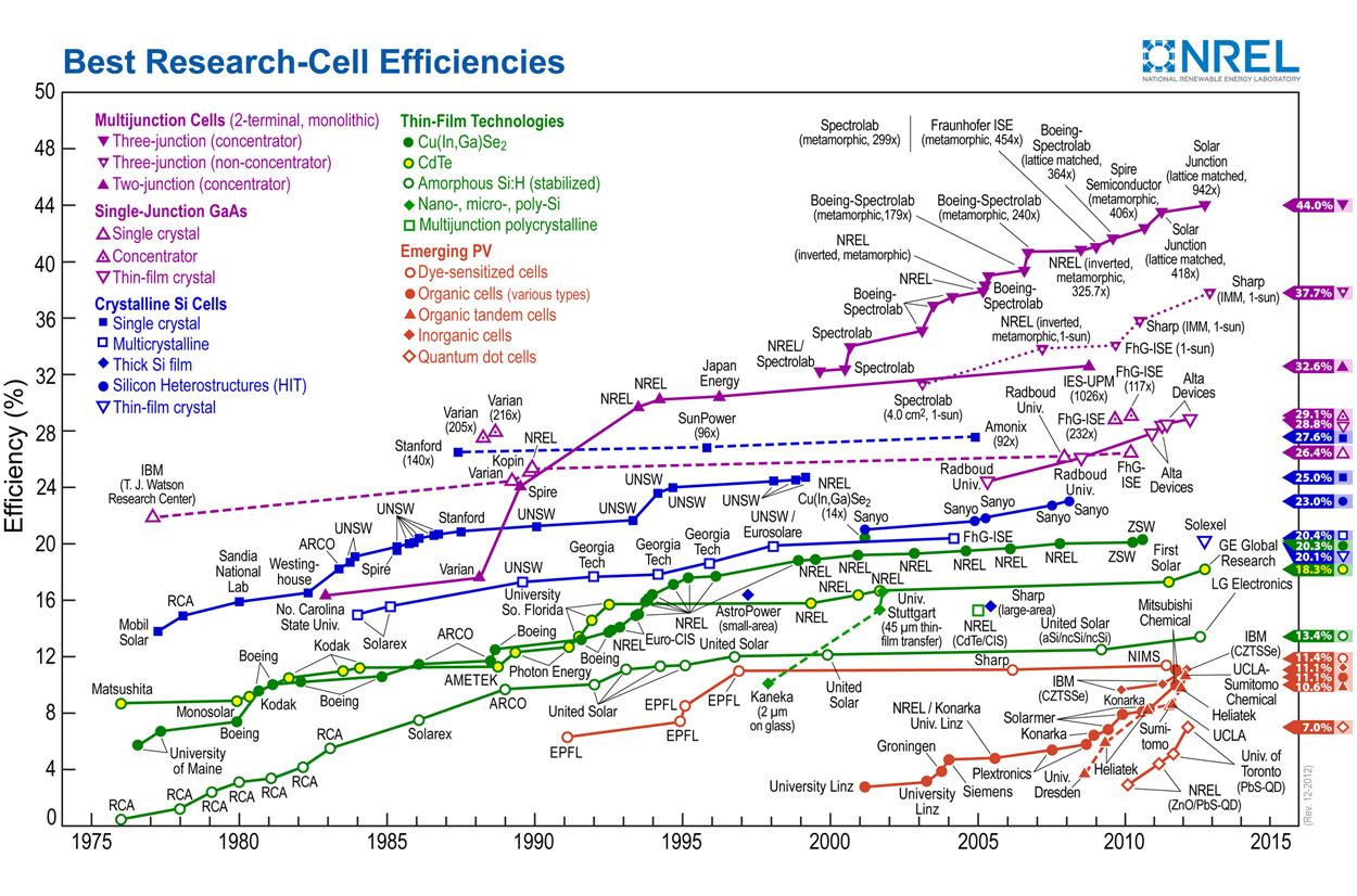