IBM creates the world’s first 2 nm chip
Posted: Thu May 27, 2021 8:49 pm
News from May 7th (before the current iteration of the forum)
IBM creates the world’s first 2 nm chip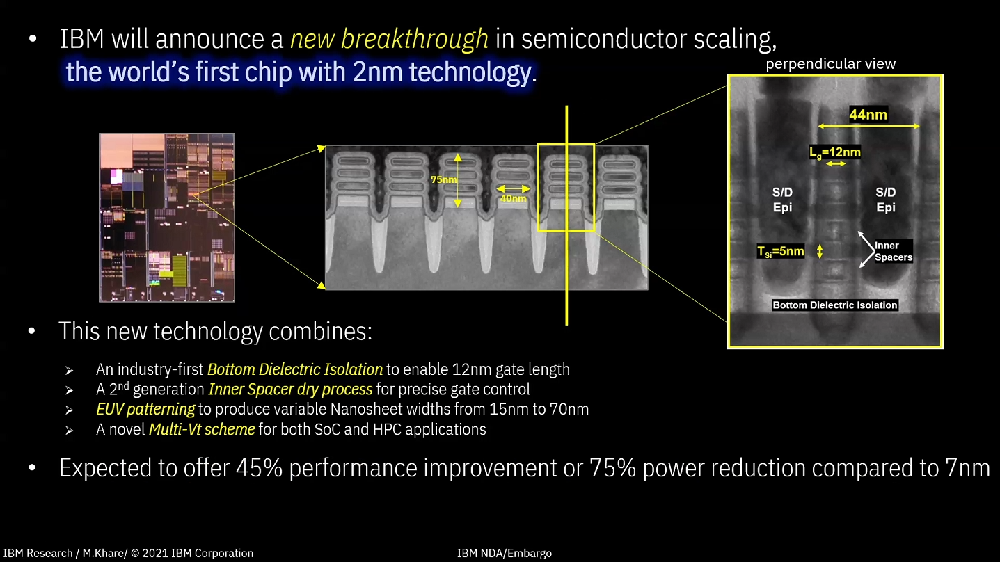
IBM creates the world’s first 2 nm chip
On Thursday, IBM announced a breakthrough in integrated circuit design: the world's first 2 nanometer process. IBM says its new process can produce CPUs capable of either 45 percent higher performance or 75 percent lower energy use than modern 7 nm designs.
If you've followed recent processor news, you're likely aware that Intel's current desktop processors are still laboring along at 14 nm, while the company struggles to complete a migration downward to 10 nm—and that its rivals are on much smaller processes, with the smallest production chips being Apple's new M1 processors at 5 nm. What's less clear is exactly what that means in the first place.
Originally, process size referred to the literal two-dimensional size of a transistor on the wafer itself—but modern 3D chip fabrication processes have made a hash of that. Foundries still refer to a process size in nanometers, but it's a "2D equivalent metric" only loosely coupled to reality, and its true meaning varies from one fabricator to the next.
To get a better idea of how IBM's new 2 nm process stacks up, we can take a look at transistor densities, with production process information sourced from Wikichip and information on IBM's process courtesy of Anandtech's Dr. Ian Cutress. Cutress got IBM to translate "the size of a fingernail"—enough area to pack 50 billion transistors using the new process into 150 square millimeters.