25th January 2019 Breakthrough in fabricating nanochips In the quest for smaller, faster 2D processors, researchers have developed a new thermal lithography process with potential for mass production at higher quality and lower cost.
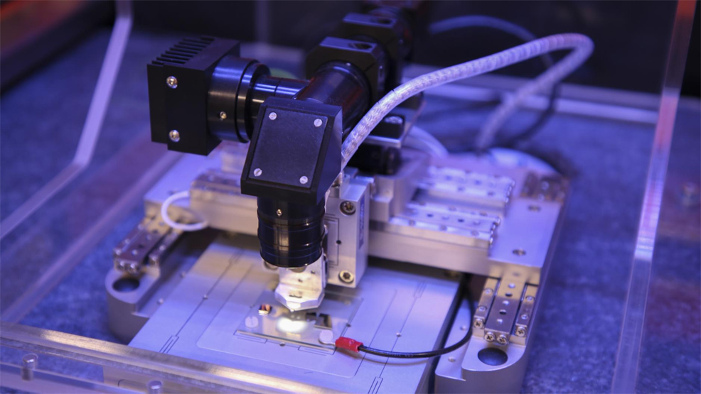
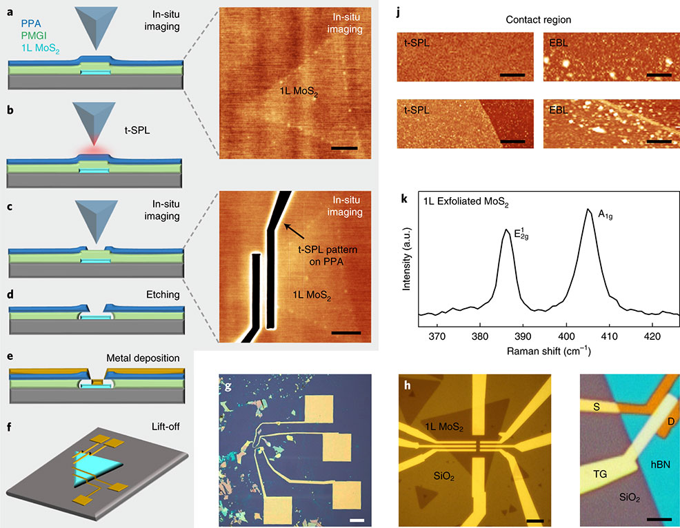
An international team of researchers has reported a breakthrough in fabricating atom-thin processors – a discovery that could have far-reaching impacts on nanoscale chip production and in labs across the globe where scientists are exploring 2D materials for ever-smaller and faster semiconductors. The team, led by New York University Tandon School of Engineering Professor of Chemical and Biomolecular Engineering Elisa Riedo, outline their research in the latest issue of Nature Electronics. Riedo and colleagues found that lithography using a probe heated above 100 degrees Celsius outperformed standard methods for fabricating metal electrodes on 2D semiconductors such as molybdenum disulfide (MoS2). Such transitional metals are among the materials that scientists believe may replace silicon for atomically small chips. The new fabrication method – called thermal scanning probe lithography (t-SPL) – offers a number of advantages over today's electron beam lithography (EBL). First, thermal lithography significantly improves the quality of the 2D transistors, offsetting the Schottky barrier, which hampers the flow of electrons at the intersection of metal and the 2D substrate. Also, unlike EBL, the thermal lithography allows chip designers to easily image the 2D semiconductor and then pattern the electrodes where desired. Furthermore, t-SPL fabrication systems promise significant initial savings as well as operational costs: they can dramatically reduce power consumption by operating in ambient conditions, eliminating the need to produce high-energy electrons and to generate an ultra-high vacuum. Finally, this thermal fabrication method can be easily scaled up for industrial production by using parallel thermal probes. Riedo hopes that t-SPL will take most fabrication out of scarce clean rooms – where researchers must compete for time with the expensive equipment – and into individual laboratories, where they could rapidly advance materials science and chip design. Someday these tools, with sub-10 nanometre resolution, running on standard 120-volt power in ambient conditions, could become ubiquitous in research labs.
Comments »
If you enjoyed this article, please consider sharing it:
|