22nd March 2021 Artificial neurons are smaller and more energy efficient Researchers at the University of California San Diego have developed a new device able to run neural network computations using 100 times less energy and area than existing CMOS-based hardware.
Training neural networks to perform tasks – such as recognising images or navigating self-driving cars – could require less computing power and hardware in the near future, thanks to a new artificial neuron device. Researchers at the University of California San Diego (UCSD) report their breakthrough in a paper published by Nature Nanotechnology. As illustrated above, neural networks are connected layers of artificial neurons, where the output of one layer provides input to the next. Generating that input is done by applying a mathematical calculation called a non-linear activation function. This is a complex process that requires a lot of computing power and circuitry as data is transferred between memory and an external processor. However, a team at UCSD has now developed a nanoscale device that can perform the activation function with extremely high efficiency. "Neural network computations in hardware get increasingly inefficient as the neural network models get larger and more complex," said corresponding author Duygu Kuzum, Associate Professor of Electrical and Computer Engineering. "We developed a single nanoscale artificial neuron device that implements these computations in hardware in a very area- and energy-efficient way."
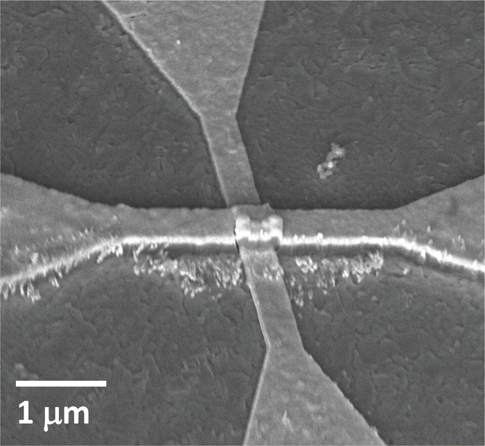
The device implements one of the most commonly used activation functions in neural network training, called a rectified linear unit. This requires hardware that can undergo a gradual change in resistance. The UCSD team engineered and optimised their device to gradually switch from an insulating to a conducting state, with help from a small amount of heat. This switch, known as a Mott transition, takes place in a nanometres-thin layer of vanadium dioxide. Above this layer is a nanowire heater made using titanium and gold. When current flows through the nanowire, the vanadium dioxide slowly heats up – causing a gradual, controlled switch, from insulating to conducting. "This device architecture is very interesting and innovative," said co-author Sangheon Oh, a PhD student in Kuzum's lab. Typically, materials in a Mott transition experience an abrupt switch from insulating to conducting because the current flows directly through the material, he explained. "In this case, we flow current through a nanowire on top of the material to heat it and induce a very gradual resistance change." The team performed tests by integrating an array of these activation (or neuron) devices with a synaptic device array, connected on a circuit board to create a hardware version of a neural network. They used the network to perform "edge detection" image processing, which demonstrated convolution operations that are essential for many types of deep neural networks – but in this case, with 100 times less energy and area than existing CMOS-based hardware. While currently a small-scale prototype, the researchers say their technology could be further scaled up to do more complex tasks. Examples might include facial and object recognition for robots or self-driving cars. "Right now, this is a proof of concept," said Kuzum. "It's a tiny system, in which we only stacked one synapse layer with one activation layer. By stacking more of these together, you could make a more complex system for different applications."
Comments »
If you enjoyed this article, please consider sharing it:
|