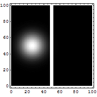
20th March 2022 Transistor gate is just 0.3 nm long Using graphene and molybdenum disulphide, scientists in China have made a transistor gate with a length of only 0.3 nanometres, equivalent to just one carbon atom, by exploiting the vertical aspect of the device. In 1959, scientists at Bell Labs invented the metal–oxide–semiconductor field-effect transistor (MOSFET). This led to mass-production of transistors for a wide range of applications – including computer processors. The Intel 4004, the first commercially produced microprocessor, debuted in 1971 and featured 2,250 transistors on a single chip, using a 10,000 nm (10 µm) fabrication process. Since that time, the MOSFET has become the most widely manufactured device in history. Thanks to vast improvements in miniaturisation, the latest processors now contain 114 billion transistors, making them 50 million times more powerful than the Intel 4004. However, this technology is becoming a victim of its own success. Transistors of today are so unimaginably tiny, many industry analysts believe they are approaching fundamental physical limits. For instance, quantum tunnelling is a problem at 7 nanometres (nm) and below, a phenomenon that causes electrons to flow through barriers meant to stop them. This can be seen in the following GIF animation, in which a ghostly spot on the right represents tunnelling electrons:
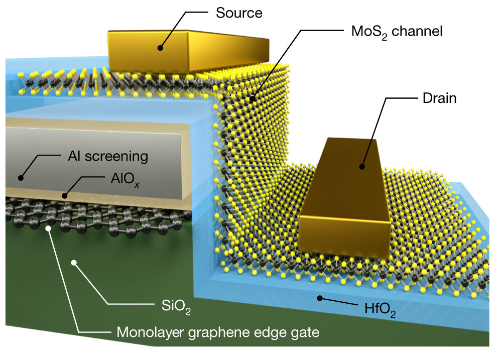
Researchers have been developing workarounds to address this and other problems, using new materials and architectures. Transistors with gate lengths of 1 nm and even less have already been achieved in the laboratory. Last year, scientists created a device just 0.65 nm in length. Now, a team at Tsinghua University, China, has built a transistor gate with dimensions as small as 0.34 nm, the size of a single carbon atom. They report this astonishing breakthrough in the journal Nature. Transistors work by sending currents from a "source" to a "drain". That flow is controlled by a gate, which switches on and off in response to an applied voltage. Silicon is no longer able to control the flow of electrons from sources to drains, due to the quantum tunnelling effect mentioned earlier. Scientists have therefore been experimenting with two-dimensional materials including graphene, which consists of single layers of carbon atoms. For this new study, researchers used a monolayer graphene edge gate and then combined it with molybdenum disulphide (MoS2), which is made of a sheet of molybdenum atoms sandwiched between two layers of sulphur atoms. Underneath the molybdenum disulphide is a thin layer of electrically insulating hafnium dioxide.
"The approach uses large-area graphene and molybdenum disulphide (MoS2) films grown by chemical vapour deposition for the fabrication of side-wall transistors on a 2-inch wafer," the researchers write. "Simulation results indicate that the MoS2 side-wall effective channel length approaches 0.34 nm in the On state and 4.54 nm in the Off state. This work can promote Moore's law of the scaling down of transistors for next-generation electronics." This device is still at the early concept stage. The team will need to show that their method can be scaled up – enabling hundreds of billions, or even trillions of transistors to work flawlessly and combine into a single processor. That is before they can even begin to consider mass production and commercialisation. Materials like molybdenum disulphide remain expensive and challenging to develop in 2D. "We have realised the world's smallest gate-length transistor," said Tian-Ling Ren, senior study author and an electrical engineer at Tsinghua University in Beijing. "The next goal is making a 1-bit CPU." Although much more research is needed, this breakthrough proves that 0.34 nm transistors are at least technically plausible. With further refinement and reductions in cost, the exponential growth in transistor counts for smartphones, laptops and other consumer electronics may continue during this decade and possibly beyond. Moore's law could once again get a reprieve, in spite of the naysayers. However, subsequent generations may be faced with a truly insurmountable hurdle in terms of miniaturisation. After all, how could transistor dimensions get any smaller than a single atom? Futurists such as Ray Kurzweil have speculated that picotechnology – orders of magnitude below nanotechnology – might be possible in 50 years or so, based on the historical trend in device sizes. But such an advance would likely require some fundamentally new understanding of physics.
Comments »
If you enjoyed this article, please consider sharing it:
|