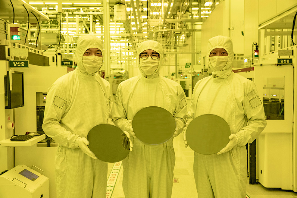
4th July 2022 Samsung begins chip production using 3 nm process Samsung has announced the first mass production of computer chips using a 3 nanometre (nm) process.
South Korean electronics giant Samsung has beaten its rival, Taiwan Semiconductor Manufacturing Company (TSMC), in the race to mass produce the world's first chips based on a 3 nm process. Multi-Bridge-Channel FET (MBCFET), a new gate-all-around (GAA) transistor architecture developed by Samsung, overcomes the performance limitations of the earlier FinFET design. It utilises nanosheets with wider channels, which allow higher performance and greater energy efficiency compared to GAA technologies using nanowires with narrower channels. The channel width of the nanosheet can be adjusted to tweak power usage and performance depending on various customer needs. Two versions of 3 nm chips are being launched. The first generation, currently in production, reduces power consumption by 45%, improves performance by 23% and reduces area by 16% compared to 5 nm. The second generation, entering production in 2023, will reduce power consumption by 50%, improve performance by 30% and reduce area by 35%.
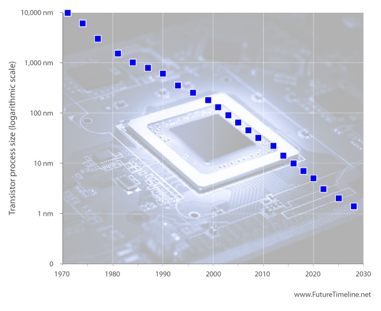
"Samsung has grown rapidly as we continue to demonstrate leadership in applying next-generation technologies to manufacturing. We seek to continue this leadership with the world's first 3 nm process with MBCFET," said Dr. Siyoung Choi, President and Head of Foundry Business at Samsung Electronics. "We will continue active innovation in competitive technology development and build processes that help expedite achieving maturity of technology." Samsung will produce the new chips at its Hwaseong and Pyeongtaek facilities, south of the South Korean capital Seoul. This announcement comes amid the ongoing global chip shortage, caused by the COVID-19 pandemic, the China–United States trade war, and various severe weather incidents. Last year, the company announced it would make a 171 trillion KRW ($132 billion) investment in the logic chip and foundry business by 2030. It also plans to establish a $17 billion semiconductor plant in Texas, its biggest investment in the U.S. and the largest foreign direct investment in the state. Following the milestone of 3 nm, both Samsung and its rival TSMC have plans for a 2 nm process by 2025. The next generation of chips after that is likely to be 1.4 nm in 2028, which could see the first consumer-level chips with over a trillion transistors.
Comments »
If you enjoyed this article, please consider sharing it:
|