
28th March 2015 10TB solid state drives may soon be possible An innovative new process architecture can extend Moore's Law for flash storage – bringing significant improvements in density while lowering the cost of NAND flash.
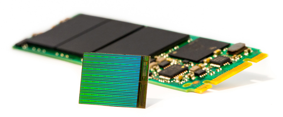
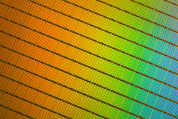
Intel Corporation – in partnership with Micron – have announced the availability of 3D NAND, the world's highest-density flash memory. Flash is the storage technology used inside the lightest laptops, fastest data centres, and nearly every cellphone, tablet and mobile device. 3D NAND works by stacking the components in vertical layers with extraordinary precision to create devices with three times higher data capacity than competing NAND technologies. This enables more storage in a smaller space, bringing significant cost savings, low power usage and higher performance to a range of mobile consumer devices, as well as the most demanding enterprise deployments. As data cells begin to approach the size of individual atoms, traditional "planar" NAND is nearing its practical scaling limits. This poses a major challenge for the memory industry. 3D NAND is poised to make a dramatic impact by keeping flash storage aligned with Moore's Law, the exponential trend of performance gains and cost savings, driving more widespread use of flash storage in the future.
"3D NAND technology has the potential to create fundamental market shifts," said Brian Shirley, vice president of Memory Technology and Solutions at Micron Technology. "The depth of the impact that flash has had to date – from smartphones to flash-optimised supercomputing – is really just scratching the surface of what's possible." One of the most significant aspects of this breakthrough is in the foundational memory cell itself. Intel and Micron used a floating gate cell, a universally utilised design refined through years of high-volume planar flash manufacturing. This is the first use of a floating gate cell in 3D NAND, which was a key design choice to enable greater performance, quality and reliability. The data cells are stacked vertically in 32 layers to achieve 256Gb multilevel cell (MLC) and 384Gb triple-level cell (TLC) dies within a standard package. This can enable gum stick-sized SSDs with 3.5TB of storage and standard 2.5-inch SSDs with greater than 10TB. Because capacity is achieved by stacking cells vertically, individual cell dimensions can be considerably larger. This is expected to increase both performance and endurance and make even the TLC designs well-suited for data centre storage.
Key product features of this 3D NAND design include: • Large Capacities – Triple the capacity of existing technology, up to 48GB of NAND per die, enabling 750GB to fit in a single fingertip-sized package. • Reduced Cost per GB – First-generation 3D NAND is architected to achieve better cost efficiencies than planar NAND. • Fast – High read/write bandwidth, I/O speeds and random read performance. • Green – New sleep modes enable low-power use by cutting power to inactive NAND die (even when other dies in the same package are active), dropping power consumption significantly in standby mode. • Smart – Innovative new features improve latency and increase endurance over previous generations, and also make system integration easier. The 256Gb MLC version of 3D NAND is sampling with select partners today, and the 384Gb TLC design will be sampling later this spring. The fab production line has already begun initial runs, and both devices will be in full production by the fourth quarter of this year. Both companies are also developing individual lines of SSD solutions based on 3D NAND technology and expect those products to be available within the next year.
Comments »
|


