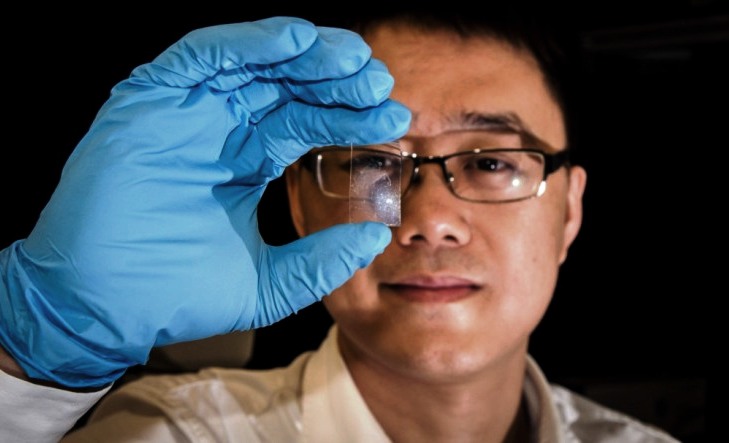
4th June 2013 Graphene sensor is 1,000 times more sensitive to light Cameras will soon take clear and sharp photos even in dim conditions, thanks to a revolutionary new sensor invented at Nanyang Technological University (NTU).
The new sensor – made from graphene – is believed to be the first to be able to detect broad spectrum light, from the visible to mid-infrared, with high photoresponse or sensitivity. This means it is suitable for use in all types of cameras, including infrared, traffic speed cameras, satellite imaging and more. Not only is the graphene sensor 1,000 times more sensitive to light than current low-cost imaging sensors found in today’s compact cameras, it also uses 10 times less energy as it operates at lower voltages. When mass produced, graphene sensors are estimated to cost at least five times cheaper. Graphene is a million times smaller than the thickest human hair (only one-atom thick) and made of pure carbon atoms arranged in a honeycomb structure. It is known to have a high electrical conductivity among other properties such as durability and flexibility. Assistant Professor Wang Qijie, from NTU’s School of Electrical & Electronic Engineering, said: “We have shown that it is now possible to create cheap, sensitive and flexible photo sensors from graphene alone. We expect our innovation will have great impact not only on the consumer imaging industry, but also in satellite imaging and communication industries, as well as the mid-infrared applications. “While designing this sensor, we have kept current manufacturing practices in mind. This means the industry can in principle continue producing camera sensors using the CMOS (complementary metal-oxide-semiconductor) process, which is the prevailing technology used by the majority of factories in the electronics industry. Therefore manufacturers can easily replace the current base material of photo sensors with our new nano-structured graphene material.”
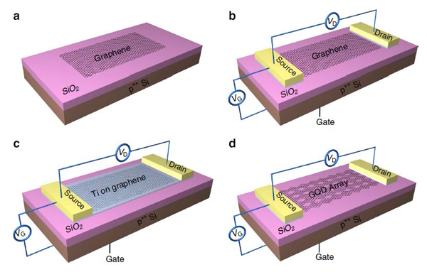
Fabrication process of the device. Credit: Y. Z. Zhang et al./Nature Communications
Asst Prof Wang came up with an innovative idea to create nanostructures on graphene which “trap” light-generated electron particles for a much longer time, resulting in a stronger electric signal. Such electric signals can then be processed into an image, like a photograph captured by a digital camera. The “trapped electrons” is key to achieving high photoresponse in graphene, which makes it far more effective than traditional CMOS or CCD (charge-coupled device) image sensors, said Wang. Essentially, the stronger the electric signals being generated, the clearer and sharper the photos. “The performance of our graphene sensor can be further improved, such as the response speed, through nanostructure engineering of graphene, and preliminary results already verified the feasibility of our concept,” he added. The research, costing $200,000, took Wang and his colleagues a total of two years to complete. The next step is to work with industry collaborators to develop the sensor into a commercial product.
Comments »
|