Researchers discover groundbreaking method to commercialise graphene for electronics
Graphene has the potential to usher in a new era of next generation electronic devices, including flexible displays and wearable technology.
Samsung Electronics have announced a breakthrough synthesis method to speed the commercialisation of graphene, a unique material ideally suited for electronic devices. Samsung Advanced Institute of Technology (SAIT), in partnership with Sungkyunkwan University, became the first in the world to develop this new method.
“This is one of the most significant breakthroughs in graphene research in history,” said the laboratory leaders at SAIT’s Lab. “We expect this discovery to accelerate the commercialisation of graphene, which could unlock the next era of consumer electronic technology.”
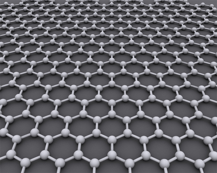
Graphene has 100 times greater electron mobility than silicon, the most widely used material in semiconductors today. It is more durable than steel and has high heat conductibility as well as flexibility, which makes it the perfect material for use in flexible displays, wearables and other next generation electronic devices.
Through its partnership with Sungkyungkwan University’s School of Advanced Materials Science and Engineering, SAIT uncovered a new method of growing large area, single crystal wafer scale graphene. Engineers around the world have invested heavily in research for the commercialisation of graphene, but have faced many obstacles due to the challenges associated with it. In the past, researchers have found that multi-crystal synthesis – the process of synthesising small graphene particles to produce large-area graphene – deteriorated the electric and mechanical properties of the material, limiting its application range.
The new method developed by SAIT and Sungkyunkwan University synthesises large-area graphene into a single crystal on a semiconductor, maintaining its electric and mechanical properties. The new method repeatedly synthesises single crystal graphene on the current semiconductor wafer scale.
Over the past several decades, the growth of the semiconductor industry has been driven by the ability to grow the area of a silicon wafer, while steadily decreasing the process node. In order to commercialise graphene to displace the industry’s reliance on silicon, it is vital to develop a new method to grow a single crystal graphene into a large area.
The research results are published in Science Magazine and ScienceExpress, one of the world’s most prestigious science journals.