5th July 2021 New chip wiring method scales down to 3nm U.S. company Applied Materials, a leading supplier of semiconductor manufacturing equipment, has revealed a new process to engineer the wiring of advanced logic chips that can scale down to 3 nanometres (nm).
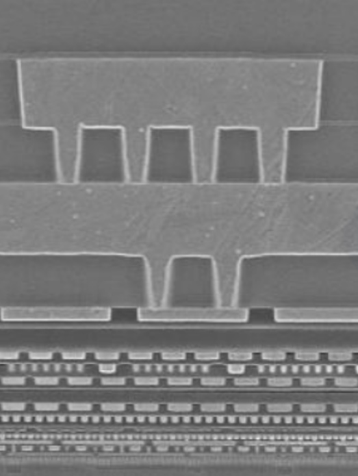
While size reduction benefits transistor performance, the opposite is true of interconnect wiring: smaller wires have greater electrical resistance, which means reduced performance and higher power consumption. Without a materials engineering breakthrough, interconnect resistance would increase by a factor of 10 from the 7nm node to the 3nm node, negating the benefits of transistor scaling. Applied Materials, headquartered in Silicon Valley, has developed a new technique called Endura Copper Barrier Seed IMS. This materials engineering solution combines seven different processes in one system under high vacuum: ALD, PVD, CVD, copper reflow, surface treatment, interface engineering and metrology. This combination replaces conformal ALD with selective ALD, eliminating a high-resistivity barrier at the via interface. It also includes copper reflow technology that enables void-free gap fill in narrow features. Electrical resistance at the via contact interface is reduced by up to 50% to improve chip performance and power consumption, enabling logic scaling to continue to 3nm and smaller. "A smartphone chip has tens of billions of copper interconnects, and wiring already consumes a third of the chip's power," said Prabu Raja, Senior Vice President and General Manager of the Semiconductor Products Group at Applied Materials. "Integrating multiple process technologies in vacuum allows us to reengineer materials and structures so that consumers can have more capable devices with a longer battery life. This unique, integrated solution is designed to accelerate the performance, power and area-cost roadmaps of our customers." The Endura Copper Barrier Seed IMS system is now being adopted by leading foundry-logic customers worldwide and may soon be used in mainstream consumer electronics products. DigiTimes is a newspaper for the computer industry in Taiwan, a country that is home to TSMC, the world's largest semiconductor company and chipset supplier to Apple. The paper suggests that Apple may use the new process for its iPhone 14 in 2022. The current generation (iPhone 12) is based on the 5nm A14 chipset. While the next generation (iPhone 13) will feature a new and upgraded A15, it will remain at 5nm. DigiTimes believes that TSMC will adopt the Applied Materials process as a way of shrinking future iPhone chips down to 3nm.
Comments »
If you enjoyed this article, please consider sharing it:
|