20th December 2021 New semiconductor design could extend Moore's Law IBM and Samsung Electronics have jointly announced a breakthrough in semiconductor design, utilising a new vertical transistor architecture that demonstrates a path to scaling beyond the nanosheet.
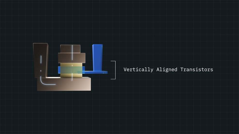
This new semiconductor design has the potential to reduce energy usage by 85% compared to current generation fin field-effect transistors (finFET) and could enable continued growth in transistor densities. Vertically aligned transistors could deliver significant improvements, including: • Cell phone batteries that last for a week or more without being charged, instead of days • Energy intensive processes, such as cryptomining operations and data encryption, requiring significantly less energy and a smaller carbon footprint • Continued expansion of the Internet of Things (IoT) and edge devices with lower energy needs, allowing them to operate in more diverse environments like ocean buoys, autonomous vehicles, and spacecraft.
"Today's technology announcement is about challenging convention and rethinking how we continue to advance society and deliver new innovations that improve life, business and reduce our environmental impact," said Dr. Mukesh Khare, Vice President of Hybrid Cloud and Systems, IBM Research. "Given the constraints the industry is currently facing along multiple fronts, IBM and Samsung are demonstrating our commitment to joint innovation in semiconductor design and a shared pursuit of what we call 'hard tech.'" Moore's Law – an ongoing trend that shows the number of transistors on a computer chip doubling every two years or so – is now approaching what are considered fundamental barriers. Simply put, as more and more transistors are crammed into a finite area, engineers are running out of space. Historically, transistors have been built to lie flat upon the surface of a semiconductor, with the electric current flowing laterally, or side-to-side, through them. Vertical Transport Field Effect Transistors (VTFET), by contrast, are built perpendicular to the surface of the chip with a vertical, or up-and-down, current flow. The VTFET process will address many barriers to performance and limitations to extend Moore's Law into the future, as chip designers are able to pack more transistors into a fixed space. It also influences the contact points for transistors, allowing for greater current flow with less wasted energy. IBM and Samsung's latest design could double a chip's performance, or reduce energy use by 85% compared to scaled finFET alternatives, with potential for even smaller scaling in the years to come.
Comments »
If you enjoyed this article, please consider sharing it:
|