6th August 2025 New 2D material outperforms future silicon chips Chinese researchers have developed the first wafer-scale, 2D indium selenide semiconductors. The resulting transistors already outperform silicon's projected performance for 2037, marking a potentially major step toward next-generation chips.
For more than half a century, silicon has served as the foundation of modern electronics. From smartphones to satellites, its consistent performance and abundance have made it the material of choice for transistors and microchips. But as demand grows for ever faster, smaller, and more energy-efficient devices, silicon is now approaching its physical limits. Transistors can only shrink so far before quantum effects and heat dissipation problems arise. Scientists around the world are therefore racing to find alternative materials that can support the next era of computing. Graphene – a single layer of carbon atoms – has long been considered a potential game-changer. Its atomic thinness and high electron mobility have attracted major interest, but difficulties in opening a bandgap for digital logic have so far limited its use in mainstream semiconductors. A bandgap is the energy barrier that electrons must overcome to conduct electricity – an essential feature for switching devices on and off. Without it, transistors cannot reliably distinguish between 1s and 0s. Other materials, such as molybdenum disulphide (MoS₂) and black phosphorus, have also shown promise, but none have yet solved the challenge of producing high-quality wafers at industrial scale. That may now be changing. In a significant advance, researchers in China have fabricated wafer-scale two-dimensional indium selenide (InSe) semiconductors, potentially paving the way for a post-silicon future. A team at the International Center for Quantum Materials, Peking University, worked in collaboration with Renmin University of China and recently published their results in Science.
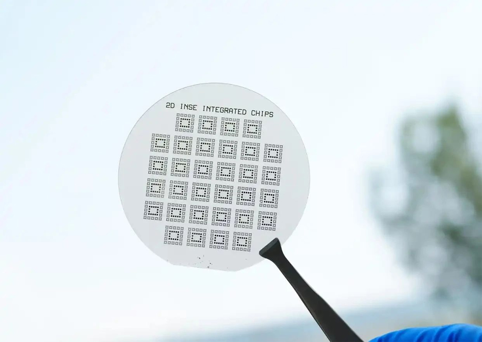
Credit: Biao Qin, et al. (Science, 2025)
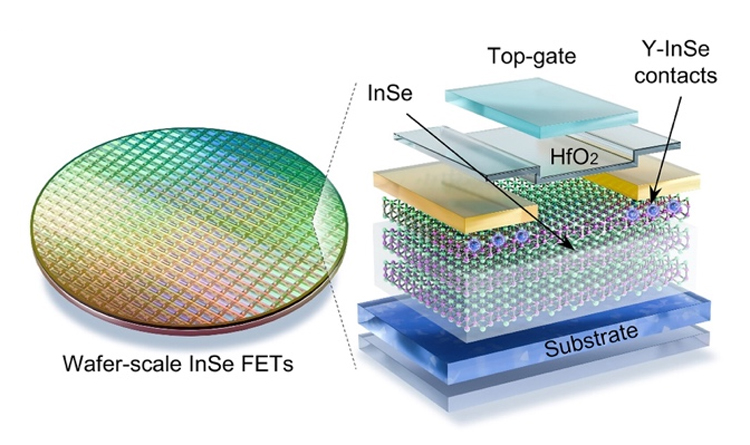
Nicknamed the "golden semiconductor", InSe combines an ideal set of characteristics: high electron mobility, low effective mass, and a suitable bandgap for transistor applications. However, scientists have struggled until now to create more than microscopic flakes – far too small and inconsistent for real-world devices. The Chinese team overcame this challenge by developing a novel "solid–liquid–solid" growth strategy. They began by depositing an amorphous InSe film onto sapphire wafers using magnetron sputtering. To initiate a reaction, they encapsulated the wafer with low-melting-point indium and sealed it inside a quartz cavity, then heated it to 550 °C. This process created a localised, indium-rich environment that triggered recrystallisation and formed a single-phase crystalline film. Through this method, the researchers produced 2-inch wafers of uniform InSe with exceptional thickness consistency and phase purity – a world first. They didn't stop there. Using these wafers, the team fabricated large-scale transistor arrays and directly compared their performance with silicon-based devices. The results were striking. The InSe transistors achieved an electron mobility of up to 287 cm²/V·s, significantly outperforming other two-dimensional materials such as molybdenum disulphide (typically below 200 cm²/V·s). Even ultra-thin silicon can struggle to maintain mobility above 200 cm²/V·s at sub-10 nm scales. The devices also demonstrated an average subthreshold swing of 67 mV/dec at room temperature – close to the theoretical minimum of 60 mV/dec, and better than the 70–100 mV/dec range seen in conventional silicon transistors. In simple terms, these values mean that InSe can switch on and off faster, while drawing less power – both crucial advantages for next-generation chip design. Already beating 2037 silicon benchmarks Crucially, the transistors also maintained strong performance at sub-10 nm gate lengths, where silicon typically suffers from leakage currents and thermal issues. Compared to performance targets from the International Roadmap for Devices and Systems (IRDS) – an annual guide to industry benchmarks – the InSe devices outperformed projections for delay and energy–delay product (EDP). EDP is a single score that multiplies the energy a transistor consumes during a switch by how long that switch takes. Remarkably, the InSe transistors already surpass the IRDS target for 2037, meaning each switch is both faster and consumes less power than what silicon is expected to achieve 12 years from now. The implications are far-reaching. With further refinement, InSe could support ultra-high-performance, low-power chips across a range of applications – from AI and autonomous vehicles to medical devices and wearable technology. Its efficiency makes it especially appealing at a time when the computing industry faces growing pressure to cut energy use. Given its unique combination of performance, efficiency, and scalability, indium selenide is now a serious contender in the race to replace silicon. As Moore's Law begins to lose momentum and the world looks beyond traditional materials, this could be a technology to watch.
Comments »
If you enjoyed this article, please consider sharing it:
|